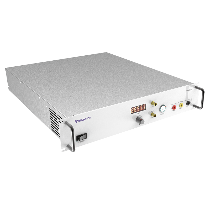
Technical Realization of High-Voltage Power Supplies in Nuclear Detection
In the field of nuclear science and technology, nuclear detection systems play a critical role in capturing, identifying, and quantifying nuclear radiation signals. As one of their core components, high-voltage (HV) power supplies serve as a vital technical foundation for achieving highly sensitive and high-resolution nuclear detection through precise energy supply and signal regulation. This article begins with the principles of nuclear detection and explores the technical implementation paths and key technical points of HV power supplies in this field.
1. Functional Positioning of HV Power Supplies in Nuclear Detection
The core principle of nuclear detection is based on the interaction between radiation particles and detection media. Common detection devices such as gas ionization chambers, scintillation counters, and semiconductor detectors all rely on HV power supplies to establish a stable electric field environment. Take gas ionization chambers as an example: HV power supplies need to form a uniform electric field with an intensity of approximately 10³-10⁴ V/m between the anode and cathode, enabling the directional migration of electron-ion pairs generated by the ionization of gas molecules by incident particles to form weak current signals (typically in the range of pA to nA) that can be collected. For semiconductor detectors, the role of HV power supplies is more specific: on the one hand, they need to provide reverse bias voltage (ranging from hundreds to thousands of volts) for PN junctions to expand the width of the depletion layer and improve charge collection efficiency; on the other hand, they need to suppress leakage current noise through precise control of the bias voltage value to ensure that the energy resolution meets the technical index of better than 1%.
2. Key Technical Realizations of HV Power Supplies
1. High-Stability Output Technology
Nuclear detection imposes extremely high requirements on the stability of HV power supplies, typically requiring the output voltage ripple to be controlled within 0.01%. This goal is achieved through multi-stage feedback control: the primary stage uses a switching power supply topology (such as flyback or LLC resonant architecture) for efficient power conversion, the secondary stage introduces a linear voltage regulator circuit (LDO) for fine voltage regulation, and a digital signal processor (DSP) is embedded to achieve adaptive PID control. For example, in a pulse amplitude analysis (PHA) system, if the power supply ripple exceeds 50mV, the channel address offset error of the multi-channel analyzer (MCA) will exceed 5%, affecting the accuracy of energy spectrum analysis. By introducing a temperature compensation network (temperature drift coefficient <50ppm/℃) into the feedback loop, the impact of environmental temperature fluctuations on output stability can be further eliminated.
2. Low-Noise Design Technology
The noise equivalent charge (NEC) of the detection system directly determines its detection threshold, making the electromagnetic compatibility (EMC) design of HV power supplies crucial. Specific technical approaches include: ① adopting an all-solid-state packaging process to integrate power devices and control circuits into a metal shielding cavity to suppress the spatial radiation of switching noise; ② configuring a π-type LC filter network (cutoff frequency <100kHz) at the input and output terminals to attenuate conducted noise; ③ optimizing the PCB layout to reduce oscillation noise caused by parasitic parameters through hierarchical design (isolation of the power layer and ground layer) and impedance matching of critical paths (characteristic impedance 50Ω±5%). Experimental data show that the HV power supply processed as above can reduce the equivalent input noise voltage density to below 10μV/√Hz, meeting the requirements of high-purity germanium (HPGe) detectors for a low-noise working environment.
3. Dynamic Response and Protection Mechanisms
The transient overloads that may occur during nuclear detection (such as breakdown currents caused by sudden changes in radiation intensity) pose challenges to the dynamic response of power supplies. To address this, a multi-layer protection architecture needs to be constructed: ① a fast current limiting circuit (response time <1μs) is activated immediately when the current exceeds 1.5 times the rated value, limiting energy injection by compressing the duty cycle through pulse width modulation (PWM); ② an overvoltage protection module uses a comparator to monitor the output voltage in real time and triggers an active discharge circuit when the voltage exceeds the set threshold (e.g., 110% of the rated voltage); ③ a thermal management system monitors the temperature rise of power devices through an integrated temperature sensor (accuracy ±0.5℃), and when the junction temperature exceeds 125℃, it activates forced fan cooling or enters a derating operation mode.
3. Typical Application Scenarios and Technological Evolution
In the field of nuclear medicine imaging, the photomultiplier tubes (PMTs) in positron emission tomography (PET) systems require ±1500V HV power supplies to provide stable operating voltages, whose stability directly affects the time coincidence accuracy of annihilation photons (required to be <5ns). In particle physics experiments, detector arrays based on microchannel plates (MCPs) require multiple independent HV power supplies (with the number of channels reaching over 64), which are remotely configured and real-time monitored through a digital power management unit (PMU) to meet the needs of multi-dimensional particle trajectory reconstruction.
In the future, HV power supply technology will develop towards integration and intelligence: power management chips based on system-on-a-chip (SoC) can achieve single-chip integration of multi-channel power supplies, and combined with software-defined power supply (SDP) technology, adaptive power configuration of detection systems can be realized through API interfaces. At the same time, the application of wide-bandgap semiconductor devices (such as SiC MOSFETs) will increase power supply efficiency to over 95% and support higher operating frequencies (>10MHz), providing technical support for the miniaturization design of compact nuclear detection equipment.