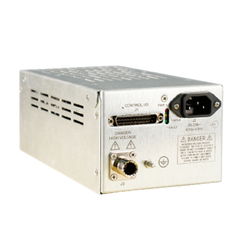
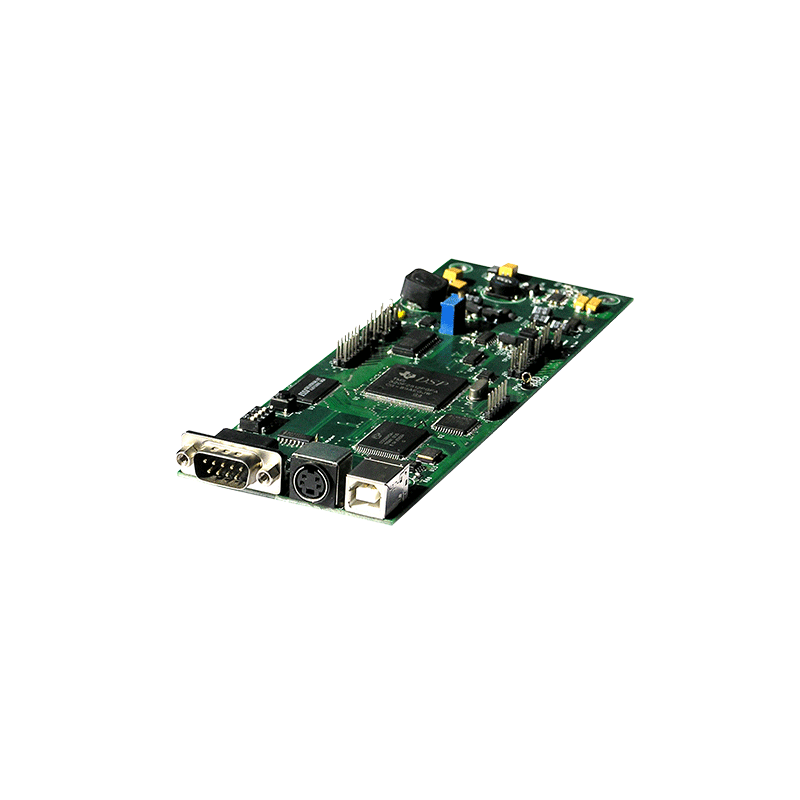
Enhanced Anti-Noise Performance of Gamma Camera Power Supply Systems
Gamma cameras, as critical devices in nuclear medicine imaging, require highly stable power systems. Power supply noise can interfere with gamma-ray detection signals, leading to image distortion or reduced signal-to-noise ratios. Enhancing noise immunity necessitates a comprehensive approach covering noise source suppression, circuit design optimization, and system-level shielding.
1. Noise Source Analysis and Suppression
Power noise in gamma cameras primarily falls into two categories:
Conducted Noise: High-frequency harmonics (MHz range) generated by switching actions (e.g., MOSFET switching), coupled via power lines to detection circuits.
Radiated Noise: Electromagnetic fields (0.15–30 MHz) from transformer leakage inductance and parasitic capacitance, disrupting weak current signals in photomultiplier tubes.
Suppression Strategies:
Transient Voltage Suppressors (TVS): Deployed at power inputs to clamp voltage spikes (e.g., 10 kV/μs) from lightning or load switching, with nanosecond response times.
Soft-Switching Technology: Achieves zero-voltage switching (ZVS) via resonant circuits, reducing switching losses by >40% and minimizing high-frequency noise.
2. Multi-Stage Filtering Circuit Design
Conducted noise paths require multi-stage filtering:
Input-Stage Filtering: π-filters (common-mode chokes + ceramic capacitors) suppress common-mode interference (150 kHz–30 MHz) with >60 dB insertion loss. Choke cores should exhibit high permeability (μ > 10,000) and low saturation.
Output-Stage Regulation: Low-dropout regulators (LDOs) combined with LC filters reduce ripple voltage to millivolt levels. Tantalum capacitors (ESR < 10 mΩ) and magnetically shielded inductors minimize radiated noise.
RC Snubbers: Parallel RC networks across switches and diodes absorb voltage oscillations from reverse recovery currents (diode recovery time < 50 ns).
3. Electromagnetic Compatibility (EMC) Optimization
Layered Shielding:
Electric Field Shielding: Copper foil between power modules and signal circuits, with ground impedance < 0.1 Ω.
Magnetic Field Shielding: Mu-metal enclosures reduce transformer flux leakage by >90%.
PCB Layout Principles:
Minimize high-frequency loop area (e.g., ≤1 cm² for switching loops), and route differential signals in parallel to reduce inductive coupling.
Dedicated layers for photomultiplier power supply to avoid ground bounce.
Low-Temperature-Drift Components: Metal-film resistors (TCR < 5 ppm/℃) mitigate DC offset from thermal drift.
4. Noise Monitoring and Dynamic Adjustment
Real-time noise spectrum analysis modules (sampling rate ≥1 GS/s) monitor power output, enabling dynamic filter tuning via FPGA:
Adaptive algorithms (e.g., LMS) suppress specific frequencies (e.g., 100 kHz switching harmonics).
Temperature sensors trigger cooling systems to limit component temperature rise to <20°C, preventing thermal noise.
> Key Table: Noise Suppression Techniques Comparison
> | Noise Type | Suppression Method | Performance Metric |
> |----------------------|------------------------------|------------------------------|
> | Conducted High-Freq | π-Filter + TVS | Insertion Loss >60 dB |
> | Radiated EMI | Mu-Metal Shielding | Flux Leakage Reduction >90% |
> | Switching Ripple | LDO + LC Filter | Ripple Voltage <5 mV |
> | Transient Spikes | Soft-Switching + RC Snubbers | Response Time <100 ns |