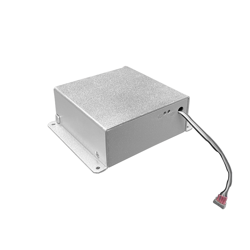
Research on Optimization of High-Voltage Power Supplies for Electrostatic Chucks
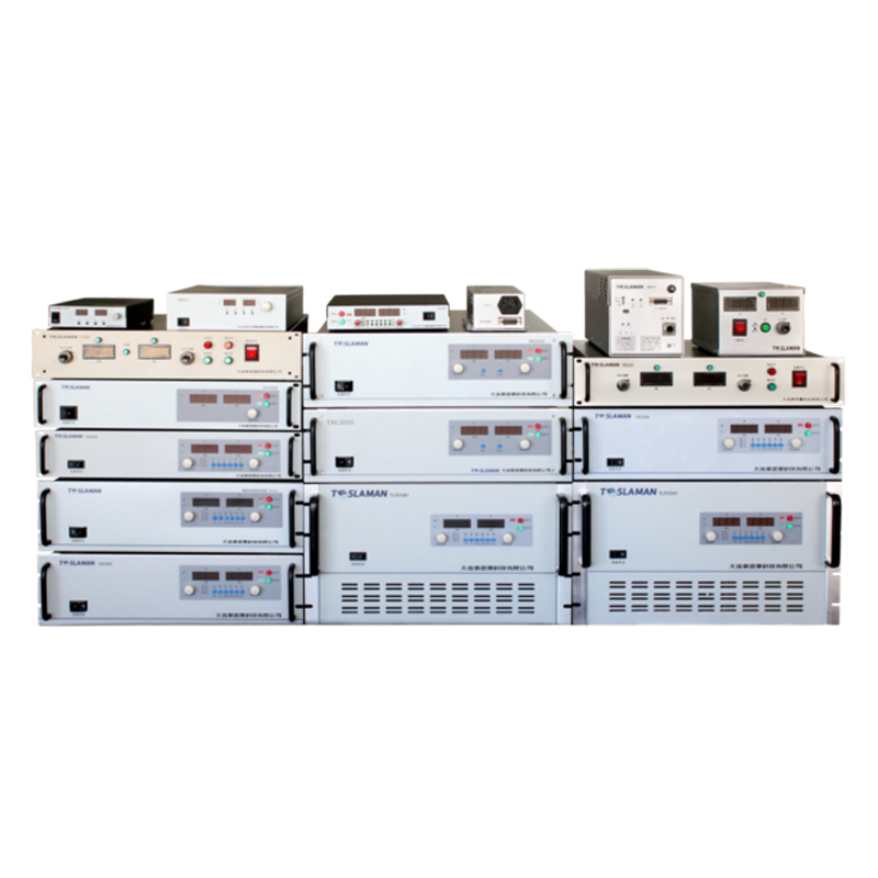
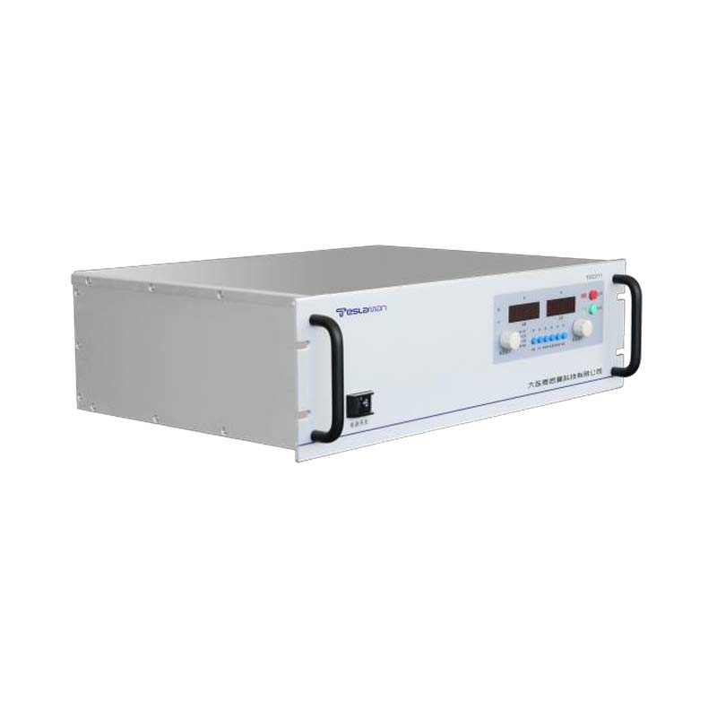
The electrostatic chuck (ESC), as a core fixture in semiconductor manufacturing, directly determines the precision and yield of wafer processing. The high-voltage power supply (HVPS), serving as the power source for electrostatic chucks, must achieve micron-level positioning and temperature uniformity (target: ±0.1°C) under extreme conditions (e.g., strong electromagnetic interference, plasma load fluctuations). This paper examines technical challenges, optimization strategies, and future directions.
I. Technical Bottlenecks
Power Stability Challenges:
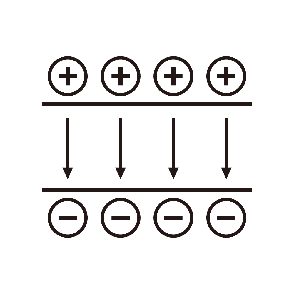
The clamping force of electrostatic chucks relies on a high-voltage electric field. Output voltage fluctuations exceeding 0.1% cause wafer displacement, leading to etching linewidth deviations (CDU > 0.5 nm). Traditional power supplies struggle to maintain stability due to electromagnetic interference (EMI > 60 dB) and load impedance variations (>300%).
Dynamic Response Lag:
Wafer processing requires millisecond-level polarity switching. Conventional power supplies with 300 ms transition times fail to meet high-speed process demands, while frequent polarity reversals risk arcing and wafer damage.
Thermal-Electric Coupling Effects:
Joule heat from electrostatic adsorption causes uneven temperature distribution, exacerbated by plasma power surges (ΔP > 500 W/s), resulting in local temperature differences > 5°C and compromising thin-film deposition uniformity.
II. Optimization Strategies and Practices
Digital Control Technology Upgrade:
Advanced Algorithms: Model predictive control (MPC) anticipates thermal load changes 300 ms in advance, while convolutional neural networks (CNN) reconstruct thermal fields with 95% compensation accuracy.
High-Frequency Response Design: Optimized switching topologies reduce voltage transition times to <10 ms and support 1 s polarity reversal, enabling high-speed processing.
Electrode Structure and Material Innovation:
Composite Electrode Arrays: Hexagonal honeycomb electrodes (200 μm main electrodes for clamping; 50 μm sub-electrodes for thermal compensation) achieve 0.08°C uniformity on 300 mm wafers (vs. 0.5°C with traditional designs).
Graded Dielectric Layers: Aluminum nitride surface layers (κ = 180 W/mK) enhance heat dissipation, while silicon nitride bases (ε_r = 7.5) suppress electric field penetration, reducing interfacial thermal resistance fluctuations.
Multimodal Thermal Management:
three-tier system is implemented: microchannel liquid cooling (±0.1 mL/min flow accuracy) for macro-scale cooling; thin-film thermoelectric coolers (TEC, <50 ms response) for regional compensation; and carbon nanotube arrays (κ = 3500 W/mK) for micro-scale conduction, slashing thermal response times from 12 s to 0.8 s.
III. Future Technical Directions
Quantum Sensing Feedback:
Diamond NV color-center sensors enable 1 μm spatial resolution and 0.01°C/√Hz temperature sensitivity, improving plasma interference resistance by 100-fold.
System-Level Integration:
Digital twin models simulating thermal-electrical-mechanical coupling predict power supply behavior under extreme conditions, shortening process development cycles by 80%.
Novel Materials Exploration:
Bioinspired thermal interface materials (anisotropic composites with κ_axial/κ_radial > 100) and photon-based thermal management (surface plasmon polariton directional heat transfer) may overcome nanoscale thermal control limitations.
Conclusion
Optimizing high-voltage power supplies is pivotal to advancing electrostatic chuck performance. Synergistic improvements in digital control, electrode design, and thermal management address stability, response speed, and temperature uniformity bottlenecks. Future integration of quantum sensing and biomimetic materials will propel semiconductor manufacturing toward atomic-scale precision.
