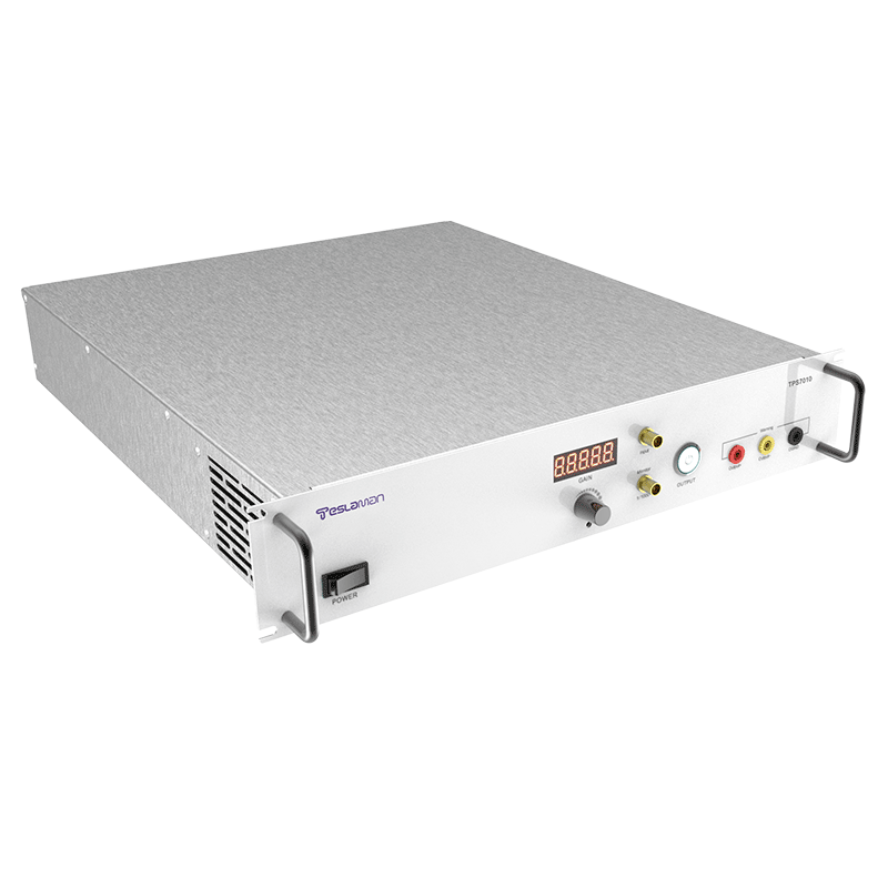
Anti-Interference Design of High-Voltage Power Supply for Lithography Machines
As the core equipment in semiconductor manufacturing, the stability of the high-voltage power supply in lithography machines directly determines exposure accuracy and chip yield. However, high-voltage power supplies are susceptible to electromagnetic interference (EMI), ground noise, and high-frequency switching noise during operation, leading to output fluctuations or system failures. Thus, anti-interference design requires a comprehensive approach encompassing power architecture, circuit layout, shielding, grounding, and software protection.
1. Power Filtering and Isolation Design
The input stage of a high-voltage power supply requires a multi-stage filtering network:
• AC Filters: Low-pass filters at the power entry point suppress high-frequency noise (e.g., surges, harmonics) from the grid, with feedthrough or three-terminal capacitors minimizing lead inductance.
• DC Decoupling: Post-rectifier parallel dual capacitors (10–100 μF electrolytic + 0.01–0.1 μF ceramic) absorb low-frequency ripple and high-frequency transients.
• Isolation Techniques: Electrostatically shielded transformers with copper foil between primary and secondary windings, single-point grounded to block common-mode noise; optocouplers isolate power and control circuits, eliminating ground loops.
2. Systematic Grounding and Shielding
• Hierarchical Grounding:
• Analog/Digital Ground Separation: Independent ground traces for analog circuits (e.g., voltage regulation) and digital circuits (e.g., PWM controllers), connected via beads or 0Ω resistors at a single point to avoid common-impedance coupling.
• Low-Impedance Grounding: Ground traces ≥2–3 mm wide with mesh layers to reduce impedance; shields, chassis, and safety grounds use short, thick wires (yellow-green) with resistance <4 Ω.
• 3D Shielding:
Enclosed metal shields for high-voltage modules, with local ferrite rings for high-frequency components (e.g., switches); twisted-pair shielded cables suppress radiated noise, with shield layers grounded at both ends.
3. EMC-Optimized PCB Layout
• Layered Stackup: 4+ layer PCBs with dedicated power and ground layers provide low-impedance return paths; high-voltage traces (e.g., switches to transformers) ≤15 mm long, avoiding 90° bends.
• Near-Field Decoupling: 0.1 μF ceramic capacitors placed adjacent to IC power pins, with via-in-pad connections to minimize lead inductance.
• Sensitive Zone Isolation: Clock circuits and oscillators spaced ≥10 mm from high-voltage areas, surrounded by ground traces; digital and high-voltage traces cross vertically to reduce mutual coupling.
4. Software-Hardware Co-Protection
• Watchdog and Monitoring: Hardware watchdogs detect power controller status, triggering resets during anomalies; ADC channels incorporate digital filters (e.g., median + moving average) to suppress transient noise.
• Logic Verification and Redundancy: Critical commands (e.g., exposure triggers) use triple modular redundancy; communication protocols add CRC checks and retransmission to prevent data corruption.
Conclusion
The anti-interference design of high-voltage power supplies for lithography machines requires a four-tier defense of isolation-filtering-shielding-grounding, supported by multi-layer PCB layouts and software fault tolerance. As lithography precision advances to nanometer levels, future research must focus on active high-frequency magnetic field cancellation and wide-bandgap semiconductor devices (e.g., SiC) to address EMI challenges at higher power densities.