Adaptive Pulse Modulation in High-Voltage Power Supplies for Ion Implantation: A Breakthrough in Precision Manufacturing
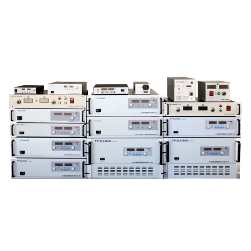
In semiconductor manufacturing, material surface modification, and advanced medical equipment, ion implantation technology is a core process for tuning material properties. Its central challenge lies in precisely controlling ion energy, depth, and spatial distribution. Traditional high-voltage power supplies face issues such as excessive pulse fall time (up to 150μs), high energy consumption, and delayed response, leading to increased low-energy ion contamination (∼24%) during implantation, which causes sputtering effects and non-uniform layer depth. Adaptive pulse modulation technology has revolutionized this process through dynamic response to load variations, millisecond-level pulse parameter correction, and energy-optimized design.
1. Technical Challenges and Core Innovations of Adaptive Mechanisms
• Steep Fall-Edge Control
Prolonged pulse fall time results in slow residual charge dissipation, generating low-energy ions that degrade layer uniformity. Adaptive modulation employs a pull-down IGBT series switch that activates immediately after the vacuum tube turns off, rapidly discharging residual charge from load and parasitic capacitors through current-limiting resistors. This reduces fall time from 150μs in conventional systems to under 5μs. For instance, 100kV-level power supplies achieve a rise time of 2–3μs, significantly minimizing low-energy ion contamination.
• Dynamic Load Matching
Plasma impedance fluctuates with real-time changes in gas pressure and temperature. Adaptive systems use real-time current/voltage monitoring combined with pre-trained algorithms (e.g., machine learning models) to dynamically adjust pulse width, frequency, and amplitude. In multi-layer implantation, voltages (hundreds of volts to hundreds of kilovolts) switch within milliseconds, ensuring each layer’s energy precisely matches target depths.
• Energy Consumption Optimization
Traditional systems waste >30% of power on charging current-limiting and pull-down resistors. Adaptive technology replaces resistors with IGBT series switches and high-frequency resonant topologies (e.g., CLLC circuits), slashing energy loss to one-fifth of conventional levels while boosting efficiency to 96.5%. The pull-down IGBT conducts only during discharge, eliminating continuous power dissipation.
2. Cutting-Edge Technological Innovations
• Third-Generation Semiconductor Devices: Silicon carbide (SiC) components withstand high voltages (1200V) with low switching losses, enabling nanosecond-level pulse modulation and enhanced noise immunity (CMTI >200kV/μs) for signal integrity in high-voltage environments.
• AI-Driven Parameter Optimization: Microprocessors analyze beam current and plasma states in real time, with AI algorithms predicting load fluctuations to dynamically adjust outputs. For example, voltage stability (fluctuation <±0.05%) recovers within 20μs upon detecting ion source instability.
• Topology Innovations: Magnetically integrated multi-phase topologies (e.g., totem-pole PFC + phase-shifted full bridge) combine fast response with low ripple (<1‰). At 30kV output, ripple noise is constrained to 100ppm, preventing ion energy drift-induced depth deviations.
3. Expanding Application Scenarios
• Advanced Semiconductor Processes: For sub-3nm chips, adaptive power enables multi-layer heterojunction implantation, ensuring transistor threshold voltage deviation <0.1% and higher yield.
• Medical Precision Therapy: In intravascular lithotripsy (IVL), high-voltage pulses (2–4kV) modulated adaptively generate ≥5MPa targeted shockwaves, fragmenting calcified plaques with <0.1mm error.
• Aerospace Material Modification: Nitrogen ion implantation on titanium alloys uses tunable ion energy (1–10keV) to form nano-hardened layers, increasing wear resistance by 300%.
4. Future Trends: From Static Settings to Intelligent Collaboration
Next-generation technology will integrate quantum control and edge computing: Quantum sensors capture plasma density in real time, while edge-deployed AI computes optimal pulse sequences, enabling closed-loop power-plasma control. Topologies will evolve toward ultra-high-frequency soft switching (>10MHz), compressing response time to nanoseconds for extreme applications like quantum devices and fusion energy systems.
Conclusion
Adaptive pulse modulation redefines the performance boundaries of ion implantation power supplies. By addressing core challenges—steep fall-edge control, dynamic load matching, and AI optimization—it eliminates low-energy ion contamination, energy waste, and process drift. Its value extends beyond semiconductor manufacturing’s nanoscale precision to disruptive applications in healthcare and aerospace. As SiC devices and intelligent algorithms converge, high-voltage power supplies are evolving from mere energy providers to process enablers, ushering precision manufacturing into an adaptive era.
