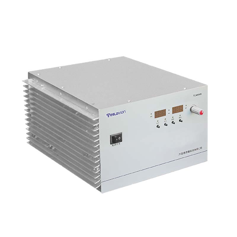
Intelligent Temperature Compensation Technology for Ion Implantation High-Voltage Power Supplies
1. Temperature Sensitivity of Ion Implantation Processes
Ion implantation is a core semiconductor manufacturing process that bombards chip surfaces with high-energy ion beams to form doped regions. This process is highly temperature-sensitive:
• Beam Current and Energy Effects: High beam currents (>120 μA) or energies (>200 keV) significantly increase surface temperature. Experiments show that every 10 μA increase in current raises temperature by 5–15°C (at 0°C cooling), while increasing energy from 150 keV to 300 keV elevates temperature by 6–14°C.
• Thermal Conduction at Interfaces: Roughness of the contact surface between the chip and silicon carrier directly affects heat dissipation. A 5 μm roughness variation can cause local overheating, leading to photoresist deformation and mask failure.
2. Multifaceted Impacts of Temperature Fluctuations
Uncontrolled temperature causes critical issues:
• Enhanced Lattice Damage: High-temperature ion bombardment displaces lattice atoms, breaking Hg-Te bonds (in HgCdTe) and generating interstitial Hg atoms. These defects are difficult to repair during annealing, increasing PN junction leakage current. For example, devices implanted at 85°C exhibit 86% higher reverse current (14.9 nA) than those at 0°C (8 nA).
• Dopant Profile Diffusion: High temperatures promote lateral diffusion of implanted atoms, causing actual junction depths to deviate from design values. In HgCdTe implantation, effective junction depths can exceed design values by 1–3 μm, increasing turn-on voltage (83.7 mV → 117.5 mV).
• Power Supply Output Drift: Temperature variations shift parameters of internal components (e.g., sampling resistors, op-amps). A 10 ppm/℃ drift with 5°C fluctuation induces 0.05% output deviation, directly affecting ion beam energy consistency.
3. Technical Principles of Intelligent Compensation
Suppressing drift requires material innovation and dynamic control:
• Capacitor Drift Cancellation: Series-connected positive-temperature-coefficient (PTC) and negative-temperature-coefficient (NTC) capacitors in voltage divider circuits reduce net drift to ΔC/C ≈ (αΔT)²/2. When α=20 ppm/℃ and ΔT=100°C, drift decreases from 0.2% to 0.02%.
• Reference Source Compensation: Bandgap references with curvature correction limit voltage reference drift to <30 ppm/℃. Sub-surface Zener structures with laser trimming further reduce noise below 50 μVpp.
• Thermistor Networks: Thermistors in integrator circuits match capacitance drift slopes (R_T = R_0 exp(B(1/T-1/T_0)), counteracting integration errors.
4. System Implementation and Thermal Management
Intelligent compensation combines hardware and algorithms:
• Multi-Level Thermal Control Architecture:
• Material Layer: Physical isolation of power devices from temperature-sensitive components using thermal pads.
• Circuit Layer: Zero-voltage-switching (ZVS) topologies minimize switching losses and local heating.
• System Layer: Digital controllers integrate ambient temperature, power loss, and heatsink efficiency data. Fuzzy logic algorithms dynamically adjust fan speeds and heater power to stabilize chassis temperature within ±0.1°C.
• Real-Time Feedback: PT1000 platinum resistors or thermocouples at critical nodes feed data to controllers. For instance, if temperature rise exceeds 5°C/min, algorithms prioritize reducing beam current over activating cooling to avoid oscillations.
5. Conclusion and Future Directions
Intelligent temperature compensation improves output stability to 100 ppm/8 hours (acceleration electrode) and 500 ppm/8 hours (suppression electrode), meeting sub-angstrom semiconductor manufacturing requirements. Future developments include:
• Self-Sensing Thermal Control: Distributed temperature sensors with deep learning for drift prediction and dynamic parameter adjustment.
• Wide-Bandgap Semiconductors: Exploring carrier mobility of silicon carbide (SiC) devices at cryogenic temperatures to surpass silicon-based drift limits.
