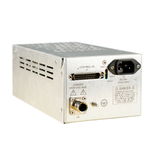
Intelligent Power Allocation for High-Voltage Power Supplies in Ion Implantation
1\. Core Requirements of Ion Implantation Processes
Ion implantation is a critical semiconductor manufacturing process that modifies material electrical properties by embedding high-energy ions into wafers. This demands high-voltage power supplies with:
• Ultra-high Stability: Output voltage fluctuation <0.1% P-P and temperature drift ≤25 ppm/℃.
• Transient Impact Resistance: Response within microseconds to ion beam transients (e.g., interruption or surge) while suppressing overvoltage/overcurrent risks.
• Long-term Reliability: Stability better than 100 ppm over 8 hours of continuous operation for 24/7 semiconductor production lines.
2\. Limitations of Conventional High-Voltage Systems
Traditional power systems face challenges in ion implantation:
• Energy Imbalance: Load fluctuations in parallel-connected units cause partial overload and low efficiency, reducing overall efficiency by 10%-30%.
• Radiation Interference: High-voltage devices under radiation induce parasitic transistor effects, increasing leakage current by 5 orders of magnitude or causing failure.
• Slow Arc Recovery: Gas breakdown (arcing) during implantation causes microsecond-scale shorts, with recovery times >100 ms, compromising process consistency.
3\. Core Technologies for Intelligent Power Allocation
3.1 Dynamic Power Reconfiguration
• Multi-module Coordination: A central controller decomposes the system into N modules and dynamically allocates power based on real-time beam demand. For example, when beam demand drops to 50%, half the modules shut down while others operate at 80% load for optimal efficiency.
• Priority Scheduling: Critical steps (e.g., gate implantation) receive 95% power, while auxiliary processes (e.g., vacuum maintenance) are limited to 30% current.
3.2 Radiation Hardening and Rapid Protection
• Channel Doping Optimization: Localized ion implantation forms a P-type doped layer along shallow trench isolation (STI) sidewalls, increasing parasitic transistor threshold voltage. Post-irradiation leakage current remains at 10⁻¹² A—5 orders lower than conventional methods.
• Arc Self-healing: Nanosecond-scale arc detection triggers immediate output cutoff and LC oscillation compensation, reducing recovery time to <20 μs with voltage fluctuation <±0.05%.
3.3 Hierarchical Energy Management
Power modes aligned with process phases:
• High-energy Implantation (>80 kV): Full-power mode with ripple suppression <0.01% P-P.
• Medium/Low-energy Implantation (<30 kV): Constant-current mode prioritizing beam uniformity.
• Standby: Modules sleep with only monitoring active, cutting power to 1% of rated value.
4\. System Implementation and Benefits
A three-tier architecture enables intelligent allocation:
1. Perception Layer: High-precision sensors (0.01% accuracy) for real-time data acquisition.
2. Decision Layer: Embedded AI chips running optimization algorithms via RS-485/EtherCAT protocols.
3. Execution Layer: IGBT+SiC MOSFET hybrid topology achieving >95% conversion efficiency.
Field data demonstrates significant improvements:
• Energy Utilization: Overall efficiency rises from 70% to 92%.
• Process Stability: Implantation depth deviation narrows from ±5% to ±1.2%.
• Equipment Lifespan: Arcing events reduced by 90%, extending power module life 3-fold.
5\. Challenges and Future Directions
Two unresolved challenges remain:
• Multi-physics Modeling: Electro-thermal-radiation coupling models are needed to optimize power allocation at >100℃.
• Nanoscale Compatibility: Sub-3nm processes require ripple <0.001%, necessitating wide-bandgap semiconductor topologies.
Future advancements will focus on:
• Digital Twin Platforms: Virtual pre-validation of power strategies to reduce trial costs.
• Green Energy Integration: Photovoltaic/storage systems for zero-carbon semiconductor fabs.
Conclusion
Intelligent power allocation for ion implantation high-voltage supplies—enabled by dynamic reconfiguration, radiation hardening, and hierarchical management—resolves critical industry pain points. As AI algorithms and wide-bandgap devices evolve, this technology will underpin sub-3nm advanced manufacturing, driving semiconductors toward ultra-precision, hyper-stability, and zero-carbon sustainability.