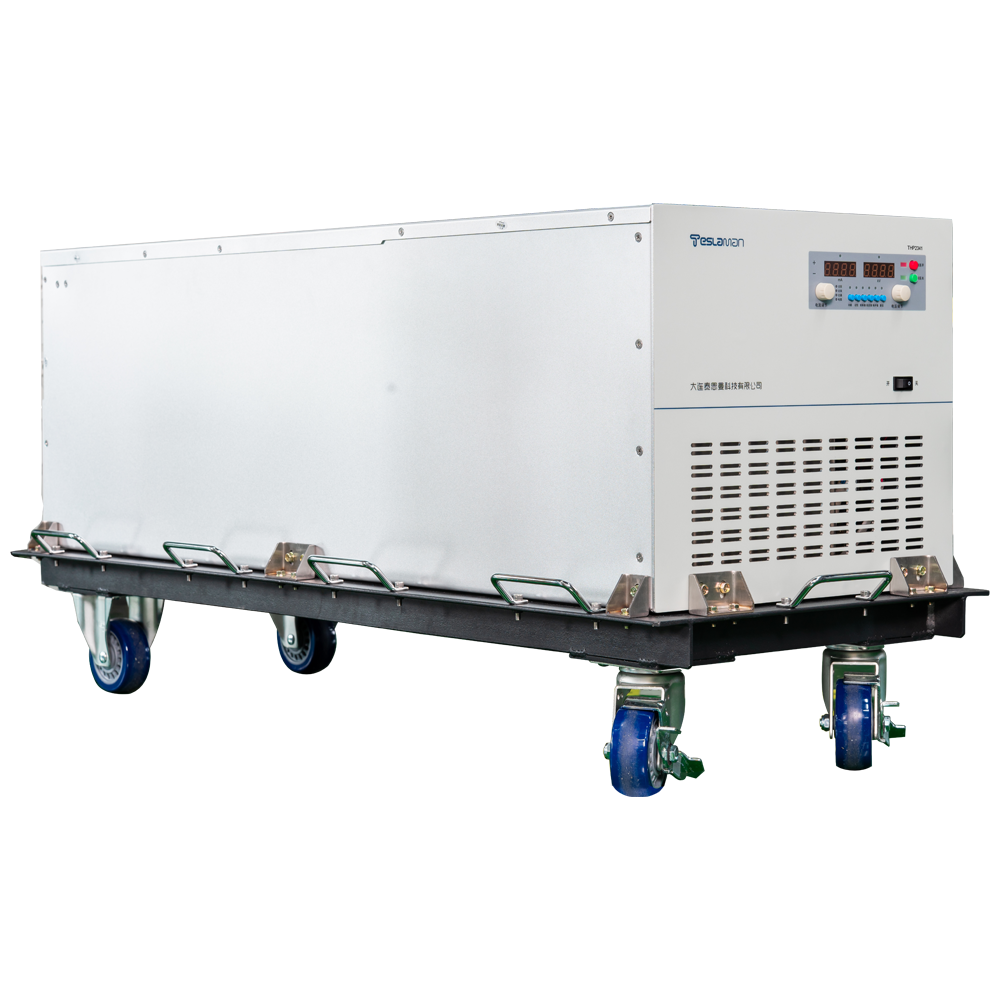
High-Voltage Power Supply for Lithography Machines: Shielding Against Particle Interference
In semiconductor manufacturing, lithography machines are core equipment for creating nanoscale circuit patterns. The stability of their high-voltage power supplies directly determines exposure accuracy and production yield. However, high-energy particles (e.g., cosmic rays, radioactive decay products) and electromagnetic interference (EMI) can cause transient voltage fluctuations, leading to wafer exposure deviations. Thus, particle-interference shielding technology for high-voltage power supplies is critical for lithography precision.
1. Hazard Mechanisms of Particle Interference
When high-energy particles penetrate equipment, they may trigger Single-Event Effects (SEE) in power supply components, causing instantaneous voltage fluctuations or logic errors. For example, charged particles striking switching transistors (e.g., MOSFETs) can activate parasitic transistors, leading to sudden output current changes and reducing servo motor positioning accuracy from ±5nm to >±20nm. Simultaneously, EMI coupled through conduction or radiation introduces noise at the output, exacerbating voltage ripple and affecting lithography layer thickness control.
2. Shielding Challenges for High-Voltage Power Supplies
Shielding must address three key conflicts:
1. Space Constraints: Supplies require ultrahigh power density (e.g., 7000W/2U), but traditional shielding increases volume.
2. Frequency Coverage: Particle interference spans broad bands (kHz to GHz), necessitating full-spectrum protection.
3. Thermal Management: Eddy currents in shielding materials increase temperature, accelerating component aging.
3. Core Technical Solutions
1. Multilayer Composite Shielding
• Inner Electric Shielding: Sensitive circuits wrapped with 0.05mm copper foil leverage the Faraday cage effect to block external fields. Copper’s conductivity (resistivity ≤0.02Ω/sq) outperforms aluminum, reducing capacitive coupling by 60%.
• Middle Magnetic Shielding: High-permeability alloys (e.g., permalloy) absorb low-frequency magnetic fields, suppressing eddy currents from transformer leakage. Tests show a 2mm-thick alloy layer attenuates 90% of sub-1kHz fields.
• Outer Particle Absorption: Tungsten-doped epoxy coatings (density ≥9.8g/cm³) block high-energy particles. Tungsten’s high atomic number (Z=74) dissipates particle energy via photoelectric effects.
2. Grounding Topology Optimization
A three-tier star grounding system separates power, signal, and shield grounds, converging at a single point with resistance <0.5mΩ. This prevents ground-loop currents and reduces common-mode noise. For long cables, cross-bonded grounding cuts sheath-induced voltage to <3V, avoiding breakdowns.
3. Dynamic Filtering and Redundancy
• Adaptive EMI Filters: Combine common-mode chokes and X2Y capacitors to dynamically compensate for load transients, limiting output voltage fluctuation to ±0.1%.
• Dual Redundancy: Primary/backup supplies switch in <10ms, ensuring zero downtime during single-event effects.
4. Application Performance
A lithography project applying these technologies achieved:
• 10,000 hours of continuous operation with zero voltage drift;
• Layer thickness control accuracy of ±0.8nm (surpassing the industry average of ±1.2nm);
• Servo motor positioning jitter below 5nm, increasing yield by 5%.
5. Future Trends
Next-gen materials like MXene titanium carbide (conductivity ≥8,000S/cm) and conductive polymer nanotubes offer lightweight, broadband shielding. Combined with AI-driven predictive maintenance, these enable real-time monitoring of shield integrity, further mitigating particle interference risks.