Dynamic Charge Balance on High-Voltage Power Supply for Electrostatic Chucks
1. Working Principle and Foundation of Dynamic Charge Balance
The electrostatic chuck (ESC), a core component in semiconductor manufacturing, utilizes a high-voltage power supply to apply DC or RF voltage to the electrode layer, generating an electrostatic field between the dielectric layer and the wafer. Free charges on the wafer’s rear redistribute under this field, creating Coulombic attraction for non-contact clamping. This process relies on dynamic surface charge balance:
• Charge Distribution Mechanism: When voltage is applied, the electrode layer’s electric field drives charge migration within the wafer, forming positive and negative charge regions. Charge density correlates positively with field strength, and adhesion follows:
\[F \propto \frac{\varepsilon V^2}{d^2}\]
where \varepsilon is the dielectric constant, V is voltage, and d is the dielectric thickness.
• Electrostatic Equilibrium: Ideally, the internal electric field should be zero (E_{\text{internal}}=0), with charges confined to the surface. However, charge distribution is influenced by wafer topography, ambient humidity, and residual contaminants, requiring dynamic regulation for stability.
2. Core Challenges in Dynamic Charge Balance
1. Non-Uniformity Interference
• Microscopic roughness or particles on wafers cause localized charge accumulation, leading to adhesion fluctuations. In plasma etching, for instance, non-uniformity may worsen, resulting in wafer displacement or thermal inefficiency.
• Environmental factors (e.g., humidity) alter surface resistivity of dielectrics, affecting charge leakage rates and disrupting balance.
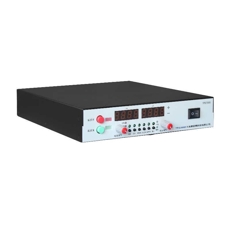
2. High-Precision Power Supply Demands
• Voltage Stability: Adhesion force is proportional to V^2. A ±5% voltage fluctuation can cause >10% force deviation, risking wafer warping. Bipolar ESCs reduce plasma dependence but require tighter voltage control (<±1% error).
• Frequency Response: Under RF bias (400 kHz–2 MHz), the power supply must rapidly adapt to plasma sheath potential changes to prevent charge buildup. Slow modulation may delay charge dissipation, inducing arcing.
3. Optimization Strategies via High-Voltage Power Technology
1. Multimodal Power Design
• DC-RF Hybrid Architecture: Pulsed voltage (e.g., 65 kV) superimposed on DC (e.g., 50 kV) accelerates charge neutralization via fast pulse edges. For example, pulsed power can increase dust removal efficiency by >30%, a principle applicable to wafer charge control.
• Adaptive Feedback Systems: Real-time monitoring of leakage current and dielectric temperature enables dynamic voltage/frequency adjustments. If localized overheating is detected, voltage reduction and backside helium cooling activate to prevent thermal stress-induced imbalance.
2. Material-Structure Co-Innovation
• High-ε Dielectrics: Materials like aluminum nitride (AlN, \varepsilon \approx 9, thermal conductivity 180 W/m·K) replace alumina, enhancing adhesion by 20% at equal voltage and improving heat dissipation.
• Micro-Electrode Arrays: Segmenting electrodes into micron-scale units with independent power modules compensates for edge charge decay, achieving <3% adhesion uniformity error.
4. Emerging Trends
1. Cryoprocess Adaptation: At ultra-low temperatures (e.g., -50°C), increased dielectric resistance slows charge dissipation. Future power supplies may integrate negative-bias pulses to force residual charge neutralization.
2. AI-Driven Predictive Models: Machine learning algorithms analyze historical process data to pre-adjust power parameters. For example, initial voltage curves can be optimized based on residual charges from prior steps.