Adaptive Resonant Frequency Control for High-Voltage Power Supplies in Lithography Systems
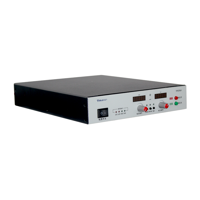
In advanced lithography systems, the stability of high-voltage power supplies (HVPS) directly determines exposure accuracy and system reliability. As lithography technology progresses toward smaller linewidths (e.g., sub-micron levels), HVPS must maintain ultra-high frequency stability (typically hundreds of kHz) at kilovolt-level voltages. However, dynamic load variations (e.g., reticle stage movement, transient plasma fluctuations) cause resonant frequency drift, leading to reduced energy transfer efficiency, increased electromagnetic interference (EMI), and even exposure defects. Adaptive resonant frequency control technology dynamically adjusts circuit parameters to keep the system operating at the optimal resonant point, serving as a core solution to these challenges.
1. Link Between Lithography Precision and Power Stability
Lithography exposure resolution relies on precise HVPS control of arc discharge or plasma excitation. For example, in proximity lithography, HVPS must generate a stable electric field within the mask-wafer gap (micron-scale). A resonant frequency deviation exceeding ±0.1% results in:
• Degraded electric field uniformity, causing linewidth variation;
• Increased EMI, disrupting high-sensitivity optical alignment systems (e.g., infrared alignment accuracy must exceed ±1.5 μm).
Traditional fixed-frequency power supplies easily detune under load changes, while adaptive technology uses closed-loop control to track the resonant point in real time, improving energy transfer efficiency to >95%.
2. Technical Challenges of Resonant Frequency Drift
The resonant frequency (f_r = 1/(2\pi\sqrt{L_r C_r}) of HVPS is perturbed by multiple factors:
• Parasitic effects: Parasitic capacitance/inductance of power devices (e.g., MOSFETs, high-frequency transformers) shifts f_r with temperature;
• Load nonlinearity: Plasma discharge impedance fluctuates within microseconds, disrupting LC resonance matching.
Without real-time compensation, voltage ripple increases by 20%–30% at light loads, while switch temperature rises accelerate at heavy loads, reducing lifespan by 50%.
3. Core Principles of Adaptive Resonance Control
The adaptive system employs a three-tier detect-compute-adjust architecture:
• Frequency detection layer: Samples resonant current phase and computes real/imaginary impedance (e.g., Z = R + j\omega L) via FPGA to identify f_r deviation;
• Dynamic tuning layer:
• Capacitor array switching: Uses HV ceramic capacitor matrices (0.1–0.4 μF range) to coarsely adjust f_r via relay switching;
• Digital fine-tuning: Adjusts PWM dead time of full-bridge inverters to modulate magnetizing inductance L_m, achieving ±2% frequency tuning;
• Closed-loop stability: Particle swarm optimization (PSO) algorithms search for optimal operating points online, with response times <100 μs—far faster than mechanical load cycles.
4. Technical Requirements for High-Frequency Stable Components
• Resonant capacitors: Metallized polypropylene film (MKP type) capacitors rated ≥3 kV with ±5% tolerance; self-resonant frequency (SRF) must exceed 10× the operating frequency to avoid high-frequency capacitive failure;
• Magnetic components: Planar transformers with nanocrystalline cores reduce eddy current losses, maintaining Q-factor >100 (@500 kHz) to ensure ZVS soft-switching at light loads;
• EMI suppression: Y2-class safety capacitors (e.g., 0.047 μF/300V~) suppress common-mode noise, minimizing interference with wafer alignment signals.
5. System Integration Challenges in Multi-Physics Fields
Within the confined space of lithography systems, HVPS must address:
• Thermo-electric coupling: A 10°C temperature rise in resonant capacitors causes 0.5% capacitance drift, necessitating thermoelectric coolers (TECs) and sensors for ±1°C thermal control;
• EMC design: Multi-layer EMI shielding suppresses radiation noise below 60 dBμV (30–300 MHz band), protecting optical systems.
6. Future Trends and Applications
Adaptive resonance technology enables higher power density in lithography:
• Wide-bandgap semiconductors: SiC/GaN devices support MHz switching frequencies, reducing power supply volume by 40% with adaptive control;
• Multi-resonant operation: Pulse loads in step-and-scan lithography drive development of multi-band resonant networks for nanosecond-scale frequency reconfiguration.
Conclusion
Adaptive resonant frequency control transforms HVPS from passive voltage stabilizers to active tuners, becoming a critical enabler for next-generation lithography. Future advancements will integrate digital twin technology to simulate load-transient scenarios and refine control algorithms, addressing the stringent demands of sub-3nm processes.