Dynamic Matching Networks for High-Voltage Power Supplies in Etching Equipment: Technology Evolution and Applications
In semiconductor manufacturing, the performance of etching equipment directly determines the precision and yield of chip structures. As process nodes advance below 5nm and wafer sizes increase to 12 inches, etching processes impose nearly stringent requirements on the stability, response speed, and power accuracy of high-voltage power supplies. The Dynamic Matching Network (DMN), as a core module of high-voltage power systems, addresses critical issues such as energy reflection and process drift caused by dynamic fluctuations in plasma load through real-time impedance matching. It has become a key technology for improving etch uniformity and selectivity.
1. Principles and Technological Evolution of Dynamic Matching Networks
Plasma density and distribution within an etch chamber are influenced by multiple factors, including gas composition, pressure, and RF power, resulting in nonlinear dynamic impedance characteristics. Traditional fixed matching networks fail to respond to load changes in real time, causing partial RF power reflection (VSWR >1.5), which reduces energy efficiency and triggers plasma instability, leading to edge over-etch or center residue. DMNs overcome this challenge through the following breakthroughs:
• High-Speed Impedance Sensing & Feedback
High-frequency voltage/current sensors (sampling rate >1MHz) monitor incident and reflected power in real time, while Smith chart analysis resolves complex impedance (real/imaginary components), completing impedance diagnosis within 10ms.
• Adaptive Tuning Algorithms
Fuzzy PID control models dynamically adjust variable capacitors/inductors in the matching network, stabilizing VSWR below 1.1, improving power transfer efficiency to >95%, and reducing reflected power loss to <2%.
• Multi-Frequency Collaborative Coupling
For high-aspect-ratio etching (>70:1) in 3D NAND, dual-frequency RF (2MHz/60MHz) synchronization is supported. Low frequencies control ion bombardment energy, while high frequencies maintain plasma density. Phase-synchronization technology prevents frequency interference, achieving vertical etch angles with <0.5° deviation.
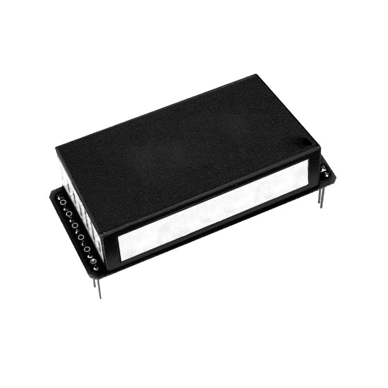
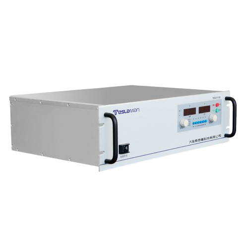
2. Technical Architecture and Key Components
The core architecture of DMNs comprises three modular layers:
• Power Conversion Layer
Full-bridge LLC resonant topology with SiC/GaN power devices increases switching frequencies to >30kHz, reducing output ripple to ≤0.1% and minimizing plasma density fluctuations.
• Impedance Actuation Layer
Vacuum variable capacitors (VVCs) and magnetic saturation inductors are integrated, with piezoelectric ceramic actuators fine-tuning capacitance (±0.1pF precision). Response times are shortened to 50μs, significantly suppressing arcing.
• Intelligent Control Layer
AI-driven compensation algorithms predict impedance trends using historical process data. For example, in metal gate etching, machine learning models preempt impedance transitions after fluorocarbon gas injection, adjusting parameters in advance to control within-wafer uniformity (WIW) within ±1.5%.
3. Process Optimization and Applications
DMNs enable precise energy control, enhancing etch outcomes for complex structures:
• High-Aspect-Ratio Etching
In deep trench etching, DMNs combined with pulsed bias technology adjust ion incident angles to 88°–90°, preventing sidewall distortion. Charge neutralization suppresses notching, enabling aspect ratios >100:1.
• Low-Temperature Etching
For 2D materials (e.g., transition metal dichalcogenides), DMNs compensate for reduced gas dissociation at -30°C, maintaining etch rate stability (<±2% variation).
• Heterogeneous Multi-Layer Etching
In GaN/SiC heterojunctions, multi-stage impedance matching switches adapt to different material selectivities, minimizing interface damage and compressing critical dimension (CD) errors to <0.2nm.
4. Future Challenges and Trends
As GAA (Gate-All-Around) and CFET (Complementary FET) architectures proliferate, DMNs face three challenges:
• Ultra-High Frequency Demands
>100MHz RF sources will become mainstream, requiring DMNs to support millimeter-wave bands while suppressing EMI.
• Multi-Physics Field Coupling
Thermal fields (wafer temperature control ±0.3°C), gas flow fields (uniformity ±3%), and plasma density fields must be co-optimized via digital twin models.
• Material Innovation
Plasma-resistant ceramic coatings (e.g., Y₂O₃-Al₂O₃ composites) are needed to extend component lifetimes beyond 1,000 hours and reduce maintenance costs.