Intelligent Gradient Boost Technology for High-Voltage Power Supplies in Ion Implantation: A New Engine for Precision Manufacturing
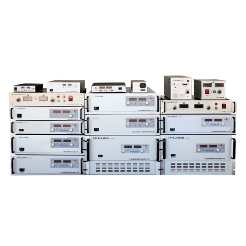
Ion implantation technology is a core process in semiconductor manufacturing, enabling precise doping of material surfaces with high-energy ion beams to tailor electrical properties (e.g., conductivity, radiation resistance). The accuracy of this process directly determines chip performance and reliability. Traditional high-voltage power supplies provide basic energy but face challenges in output stability and impurity uniformity. For instance, in radiation-hardening processes, thermal annealing after ion implantation can cause impurity redistribution, increasing device leakage current or reducing breakdown voltage.
Breakthrough Innovations in Intelligent Gradient Boost Technology
Intelligent gradient boost technology addresses the limitations of conventional power supplies through dynamic output adjustment:
1. Adaptive Energy Control: The system autonomously adjusts the boost curve slope based on real-time load conditions (e.g., ion beam intensity, target impedance). In shallow trench isolation (STI) processes, for example, gradually increasing implantation energy (e.g., from 50 keV to 120 keV) suppresses impurity diffusion during subsequent thermal steps, stabilizing ion concentration at STI sidewalls and reducing leakage current by five orders of magnitude.
2. Hybrid Topology Architecture: Combining switch-mode power supplies (Buck-Boost) with charge pumps achieves efficient energy conversion. The inductor energy storage phase (duty cycle DT) of switch-mode supplies provides base voltage elevation, while charge pumps superimpose pulsed high voltage via capacitive coupling, enabling precise µs-level voltage transitions. This design reduces energy loss by over 60% compared to traditional solutions and supports ultra-high outputs exceeding 20 kV.
3. Noise Suppression Strategy: Digital closed-loop control with real-time voltage ripple compensation ensures stability. By integrating low-pass filters and ripple-cancellation modules, the power supply restricts noise to mV levels, maintaining ion beam focus accuracy (beam spot diameter <0.1 µm).
Applications and Performance Validation
1. Radiation-Hardened Device Fabrication: In 180 nm embedded flash memory processes, intelligent gradient boost optimizes ion implantation for high-voltage NMOS devices. By relocating the hardening implantation step post-gate oxidation and confining ions to the mid-channel region, it prevents degradation of drain PN junction breakdown voltage. Post-irradiation at 1.5×10⁵ rad(Si), devices exhibit off-state leakage currents of ~10⁻¹² A, meeting aerospace-grade requirements.
2. Wide-Bandgap Semiconductor Doping: For AlGaN/GaN HEMT devices, fluorine implantation requires penetrating heterojunction interfaces to form acceptor traps. Stepwise boosting (5 kV per stage) in the source region creates uniform trap distribution in the GaN buffer layer, increasing breakdown voltage to 262 V—a 40% improvement.
3. Multi-Voltage-Domain Integration: Adaptive Power Tracking (APT) technology dynamically matches supply voltage to load demands (e.g., RF PA modules) via Buck-Boost topologies, achieving 95% system efficiency with voltage transitions completed within 10 µs.
Future Directions
Intelligent gradient boost technology will evolve toward:
• AI-Driven Predictive Control: Machine learning models will preempt parameter drift to optimize boost curves proactively.
• Cryogenic Boost Integration: Combining low-temperature techniques reduces thermal damage during implantation, enhancing dopant activation rates.
• Topology-on-Chip Miniaturization: Integrating charge pumps and inductive energy storage into single chips will enable portable nanoscale ion implantation systems.
The intelligent advancement of high-voltage power supplies for ion implantation is shifting semiconductor manufacturing from experience-driven to data-driven, laying the foundation for atomic-scale precision in next-generation chips.
