Technical Path and Application Value of Pulse Sequence Optimization for High-Voltage Power Supplies in Ion Implantation
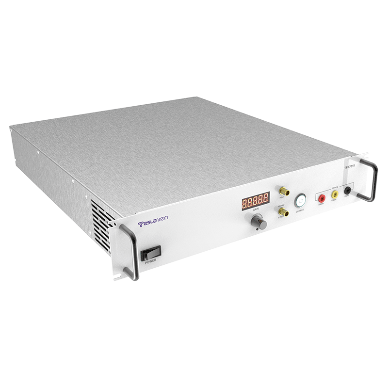
In the doping process of semiconductor manufacturing, ion implantation technology constructs the electrical characteristic regions of devices by precisely implanting specific ions into the surface layer of wafers, which is a core link determining chip performance and yield. As the energy supply core of the ion implantation system, the high-voltage power supply (HVPS) has its output pulse sequence's stability and accuracy directly related to the energy control of the ion beam and the uniformity of beam current density, thereby affecting the consistency of doping concentration and the degree of wafer lattice damage. The pulse sequence design of traditional HVPS is mostly based on fixed timing parameters, which are easily affected by factors such as load fluctuations and plasma instability, leading to problems such as pulse voltage overshoot and energy drift. It is difficult to meet the strict requirements for doping accuracy in advanced manufacturing processes (e.g., 3nm and below). Therefore, targeted optimization of the pulse sequence has become a key direction for technological breakthroughs.
The optimization of the pulse sequence needs to focus on three core dimensions: parameter coordinated regulation, dynamic feedback adaptation, and load characteristic matching. In terms of timing parameter optimization, pulse width and rise/fall time are core variables: an excessively wide pulse width will lead to prolonged interaction time between the ion beam and the wafer, exacerbating lattice thermal damage; an excessively narrow one may result in insufficient beam intensity, affecting the doping depth. Through simulation and experimental verification, controlling the rise time within the microsecond level (usually 5-10μs) can effectively suppress voltage overshoot (reduced from 15% in traditional designs to less than 5%); at the same time, the pulse period is adjusted according to the mass difference of ion types (e.g., boron ions, phosphorus ions) to ensure consistent acceleration efficiency for different ions. In addition, the introduction of a pre-pulse main pulse coordinated structure, where the pre-pulse (with an amplitude of 30%-50% of the main pulse) can stabilize the plasma sheath in advance, reducing energy fluctuations when the main pulse is applied, and improving the ion beam energy stability from ±200ppm to within ±50ppm.
The integration of a dynamic feedback mechanism is another key part of the optimization scheme. Traditional open-loop control cannot respond to load changes in real time, while a closed-loop system based on an ion beam energy monitoring module and voltage feedback can adjust the amplitude and timing of the pulse sequence in real time through PID or model predictive control (MPC) algorithms. For example, when the monitored beam current density deviation exceeds 3%, the system can fine-tune the pulse width within 10μs, ensuring that the beam uniformity on the wafer surface is controlled within ±1%, which significantly improves the doping consistency of the entire wafer. Meanwhile, for the load characteristics of different process scenarios, customized pulse sequence optimization is required: for shallow junction doping requirements, a narrow pulse high frequency sequence is adopted to reduce the ion implantation depth; for heavy doping scenarios, a wide pulse low ripple design is used to improve beam intensity while reducing energy fluctuations.
From the perspective of application effects, the optimized pulse sequence can significantly improve the comprehensive performance of the ion implantation process: in the actual production of 12-inch wafers, the doping concentration deviation is reduced from ±8% to ±3%, the wafer lattice damage area is decreased by 40%, directly reducing the time cost of the subsequent annealing process; at the same time, the energy utilization efficiency of the pulse sequence is increased by 15%, reducing the power consumption and heat loss of the HVPS and extending the service life of the equipment. In the manufacturing of advanced logic chips and power devices, this optimization scheme can meet the high-precision doping requirements and help devices break through the bottleneck of electrical performance. For example, in the source-drain region doping of FinFETs, the improvement of ion implantation accuracy can increase the device switching speed by 10% and reduce the leakage current by 20%.
In the future, as semiconductor processes move towards smaller nodes, the pulse sequence optimization of HVPS for ion implantation will further integrate AI adaptive algorithms. By real-time analyzing multi-dimensional process data (such as wafer temperature, plasma density, and voltage fluctuation), dynamic self-adjustment of pulse parameters will be realized, promoting the development of ion implantation technology towards the direction of ultimate precision high efficiency and energy saving wide scenario adaptation, and providing core technical support for high-performance chip manufacturing.