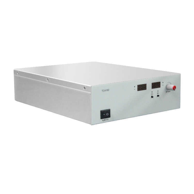
Application and Technical Value of Intelligent Dynamic Voltage Equalization for High-Voltage Power Supply of Electrostatic Chuck
In the process of semiconductor manufacturing iterating toward advanced processes of 3nm and below, the electrostatic chuck (ESC), as a core component for wafer adsorption and positioning, its performance directly determines the precision and yield of key processes such as lithography and etching. As the energy core of the electrostatic chuck, the high-voltage power supply (HVPS) has seen its traditional static voltage equalization technology become increasingly inadequate in adapting to the adsorption requirements brought by wafer thinning (thickness ≤ 50μm) and the diversification of wide-bandgap semiconductor (such as SiC, GaN) materials. Static voltage equalization can only maintain a fixed voltage output and cannot respond in real time to uneven charge distribution on the wafer surface and local potential fluctuations caused by plasma impact. This easily leads to risks such as wafer edge warping, lattice damage due to excessive central adsorption, and even breakdown of the chuck's insulating layer. Against this backdrop, the emergence of intelligent dynamic voltage equalization (IDVE) technology provides a core solution for the performance upgrade of high-voltage power supplies for electrostatic chucks.
The core logic of intelligent dynamic voltage equalization technology lies in building a closed-loop control system of real-time monitoring algorithmic regulation dynamic response. Compared with traditional technologies, its primary breakthrough is the multi-dimensional parameter sensing capability: by integrating micro-sensor arrays, it collects real-time data on the potential difference between the wafer edge and center (with a precision of mV level), the current density of chuck partitions, the real-time temperature field distribution of the wafer, and micro-deformations. This breaks the singularity of traditional voltage equalization that only relies on voltage feedback. Secondly, at the algorithm level, the adaptive PID algorithm trained based on process big data can automatically adjust the voltage compensation strategy according to the dielectric constant and thickness characteristics of different wafer materials. For example, during the etching process of SiC wafers, when it is detected that the charge density at the edge decreases due to thermal expansion, the algorithm can increase the output voltage of the corresponding area within microseconds to maintain the uniformity of adsorption force and avoid plasma undercutting the edge. In addition, this technology also has dynamic load matching capability, which can automatically optimize the voltage output curve according to the load changes in process stages (such as the exposure preparation stage of lithography and the plasma injection stage of etching), reducing energy loss while avoiding the impact of instantaneous high voltage on the wafer.
In terms of application value, intelligent dynamic voltage equalization technology brings three key improvements to semiconductor manufacturing. Firstly, it significantly enhances the stability of wafer adsorption: in the processing of 12-inch ultra-thin silicon-based wafers, after adopting this technology, the maximum warpage of the wafer is reduced from 5μm (with traditional static voltage equalization) to 1.2μm, and the contact rate of the adsorption surface is increased to 99.8%, directly solving the industry pain point of overlay precision deviation in advanced lithography. Secondly, it optimizes process consistency: by real-time compensating for the thickness deviation and surface roughness differences between wafer batches, the etching depth uniformity error of wafers in the same batch can be controlled within ±3%, and the yield is increased by approximately 8%-12%. Thirdly, it extends the service life of equipment: the dynamic adjustment mechanism avoids the aging of the chuck's insulating layer caused by local high voltage, prolonging the mean time between failures (MTBF) of the electrostatic chuck by more than 30% and reducing the maintenance cost of semiconductor production lines.
In terms of application scenario expansion, intelligent dynamic voltage equalization technology has also broken through the applicable boundary of traditional electrostatic chucks. For the wafer bonding process in 3D IC manufacturing, it can achieve differentiated adsorption of double-layer wafers by precisely controlling the layered voltage output, avoiding the generation of bubbles at the bonding interface. In the manufacturing of third-generation semiconductors, in the face of the high hardness and low thermal conductivity of SiC wafers, the technology can balance the adsorption force and heat dissipation requirements through temperature-voltage linkage regulation, reducing the cracking of wafers caused by thermal stress. As semiconductor manufacturing moves toward the direction of higher precision and wider material adaptation, intelligent dynamic voltage equalization technology is not only the performance upgrade direction of high-voltage power supplies but will also become a core technical standard for advanced process production lines, providing key support for yield improvement and cost optimization in semiconductor manufacturing.