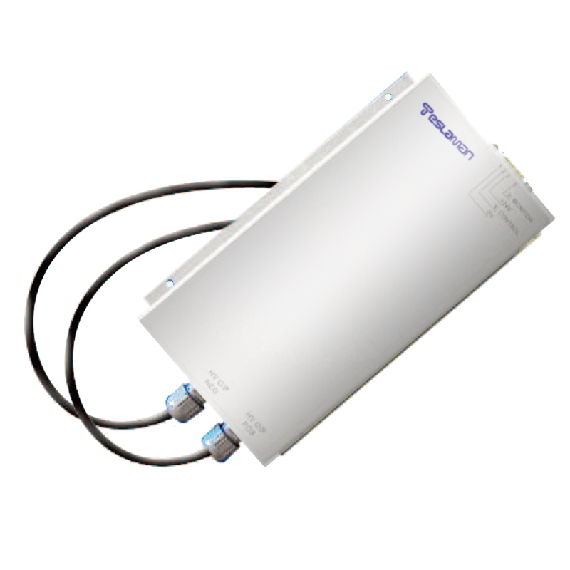
Nanoscale Surface Potential Regulation Technology of High-Voltage Power Supply for Electrostatic Chuck
In the field of precision manufacturing such as semiconductor wafer fabrication and micro-electro-mechanical systems (MEMS) processing, electrostatic chucks (ESCs) have become core components for precise positioning of ultra-thin and large-sized workpieces, thanks to their advantages of no mechanical damage and high adsorption stability. Their adsorption performance is directly related to the surface potential distribution. However, as process nodes enter the 7-nanometer (nm) and below level, the millimetric potential regulation accuracy of traditional high-voltage power supplies (HVPS) can no longer meet the strict requirements of nanoscale processing for surface flatness and positioning errors. Therefore, nanoscale surface potential regulation technology based on HVPS has become a key support for breaking through the bottlenecks of precision manufacturing.
The adsorption of ESCs essentially relies on the electrostatic field force formed by the induced charges on the electrode and workpiece surface after the HVPS applies voltage, which mainly includes two mechanisms: Coulomb force and Johnsen-Rahbek force. The Coulomb force is suitable for insulating workpieces or vacuum environments, while the Johnsen-Rahbek force plays a dominant role when there is a tiny gap between the conductive workpiece and the chuck. Regardless of the mechanism, the uniformity and stability of the surface potential directly determine the distribution of adsorption force—if the potential fluctuation exceeds 10 millivolts (mV), the difference in adsorption force will exceed 5%, leading to micro-deformation of the workpiece and nanoscale processing errors. The HVPS achieves nanoscale precision through dual regulation: on one hand, it suppresses the output voltage ripple to the microvolt (μV) level to ensure the stability of the potential reference; on the other hand, with nanosecond-level response speed, it real-time compensates for the potential drift caused by workpiece placement and ambient temperature changes, maintaining the uniformity of surface potential distribution.
Three core difficulties need to be overcome to realize this technology. The first is high-precision potential detection and closed-loop control: the surface potential of the chuck is significantly affected by vacuum degree and the dielectric constant of the workpiece. It is necessary to integrate a potential sensor at the atomic force microscope level to collect real-time distribution data and feed it back to the control unit, dynamically adjusting output parameters to control the regulation error within ±2 mV. The second is dynamic load adaptation capability: changes in workpiece size and thickness will cause fluctuations in the chuck's load impedance. The HVPS needs to adopt adaptive impedance matching technology to maintain stable output voltage even when the load impedance changes by more than 10 times, avoiding sudden potential changes. The third is stability under strong interference: radio frequency plasma and high-frequency electromagnetic radiation in precision manufacturing environments are likely to interfere with the power output. It is necessary to use multi-layer electromagnetic shielding and low-noise amplification circuits to ensure that the output voltage fluctuation does not exceed 5 μV when the interference intensity reaches 100 V/m.
This technology has significant value in precision manufacturing. In the semiconductor lithography process, it improves the uniformity of adsorption force between the wafer and the chuck to over 99.5%, reduces wafer warpage, and controls the lithography overlay error within 3 nm, meeting the needs of advanced processes. In MEMS sensor manufacturing, for silicon thin-film workpieces with a thickness of 1 micrometer (μm), precise potential regulation can avoid film rupture, increasing the yield from 85% to 98%. In the field of vacuum coating, uniform surface potential can reduce ion deflection, controlling the film thickness deviation within 2 nm and improving the transmittance stability of optical films.
The nanoscale surface potential regulation technology of HVPS is not only the core of ESC performance upgrading but also a key driver for promoting precision manufacturing towards atomic-level accuracy. As the demand for precision in high-end manufacturing continues to increase, this technology will further integrate multi-physics field analysis and AI predictive control to achieve more intelligent regulation, providing support for the performance breakthrough of high-end equipment.