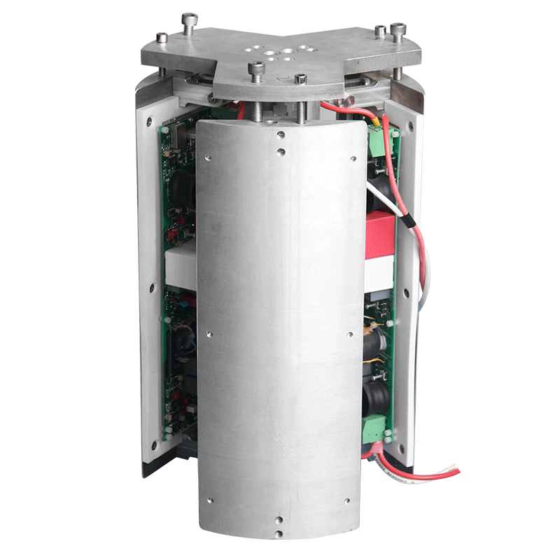
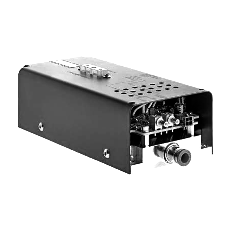
Optimization of RF-DC Coupling for High-Voltage Power Supply in Etching Equipment
In the etching process of semiconductor manufacturing, the high-voltage power supply (HVPS), as the core component for plasma generation and energy control, has its coupling performance between radio frequency (RF) and direct current (DC) signals directly determining etching precision, rate, and wafer uniformity. With the advancement of advanced manufacturing processes toward the 7nm and below nodes, the traditional RF-DC coupling method of HVPS has gradually exposed problems such as impedance mismatch, interference superposition, and energy loss. These issues lead to plasma density fluctuation exceeding ±5% and wafer etching uniformity deviation reaching 3.2%, becoming a key bottleneck restricting the improvement of process yield. Therefore, the optimization of RF-DC coupling for HVPS in etching equipment has become one of the core directions for the technological upgrading of semiconductor equipment.
The core pain points of the traditional RF-DC coupling structure focus on three dimensions: first, when the RF signal (usually 13.56MHz or 27.12MHz) and DC high voltage (hundreds to thousands of volts) share the same transmission path, energy reflection is likely to occur due to differences in impedance characteristics, resulting in a power conversion efficiency of less than 85%; second, the RF high-frequency signal will couple to the DC circuit through parasitic capacitance, causing an increase in DC output ripple, which in turn leads to instability of the plasma sheath thickness and affects the etching line width precision; third, the parasitic inductance and capacitance at the coupling node will prolong the signal response time. When the etching process requires dynamic adjustment of energy output, the power supply cannot quickly match the changes in plasma load, resulting in fluctuations in the etching rate.
To address the above problems, the optimization of RF-DC coupling needs to construct a technical solution from three aspects: topology design, interference isolation, and dynamic matching. In terms of topology optimization, a dual-path common-node design can be adopted: the RF signal and DC high voltage are transmitted to the coupling node through independent transmission channels. At the node, a multi-layer ceramic capacitor with low parasitic parameters is used as the coupling medium. While shortening the signal transmission path, the parasitic inductance is controlled below 10nH to improve the signal response speed. In terms of interference isolation, a multi-level shielding and filtering system should be built: a high-frequency choke coil is connected in series in the DC circuit to block the reverse coupling of RF signals to the DC power supply end; a band-stop filter is added in the RF path to suppress low-frequency interference introduced by DC high voltage; at the same time, a metal shield is used to wrap the coupling module to reduce the impact of the external electromagnetic environment on the coupling performance, and finally the DC output ripple is controlled within 5mV. In terms of dynamic matching, an impedance adaptive algorithm based on a digital signal processor (DSP) is introduced to collect real-time data on changes in plasma load impedance. By adjusting the LC parameters of the RF matching network and the output amplitude of the DC high voltage, the dynamic balance of RF-DC energy coupling is achieved, and the impedance mismatch coefficient is maintained below 0.1.
From the perspective of application effects, the optimized HVPS has shown significant performance improvements in the 12-inch wafer etching process: the power conversion efficiency has increased to over 92%, reducing equipment energy consumption; the plasma density fluctuation range has been reduced to ±2%, and the intra-wafer etching uniformity deviation has dropped to 1.8%, meeting the etching precision requirements of advanced processes; at the same time, the mean time between failures (MTBF) of the equipment has increased by 30%, reducing the downtime and maintenance costs of the production line. In addition, this optimization scheme has good process compatibility and can be adapted to different process requirements such as dry etching and wet etching, providing key technical support for the localization upgrade of semiconductor manufacturing equipment.
In the future, as the etching process moves toward higher precision and higher efficiency, the optimization of RF-DC coupling will also need to be combined with artificial intelligence algorithms to achieve predictive matching of load changes, further improving the dynamic response capability of HVPS and providing stable energy control support for the continuous breakthrough of advanced semiconductor manufacturing processes.