Surface Microplasma Suppression of High-Voltage Power Supply for Electrostatic Chuck (ESC)
1. Application Scenario and Cause of the Problem
The Electrostatic Chuck (ESC) is a core component for wafer clamping in semiconductor manufacturing (such as etching and thin film deposition), which realizes non-contact fixing of wafers by using the electrostatic force provided by a high-voltage power supply. However, under the clamping voltage of 10-30kV, the gap between the wafer and the chuck (usually 5-10μm) is prone to generate surface microplasma due to uneven electric field. When the gas in the gap (such as SF6 and O2 in the etching process) reaches the ionization threshold under the action of a local strong electric field (>10^6 V/m), a small discharge channel will be formed, leading to wafer surface oxidation, metal contamination or pattern damage, which seriously affects the chip yield.
2. Microplasma Suppression Technical Scheme
1.Control of Electric Field Uniformity
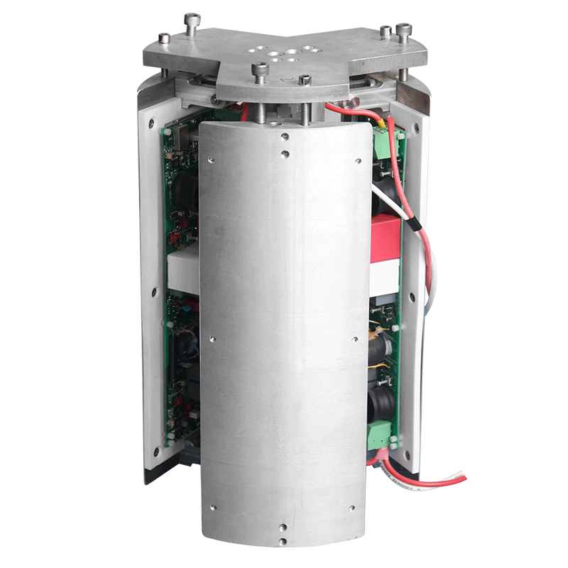
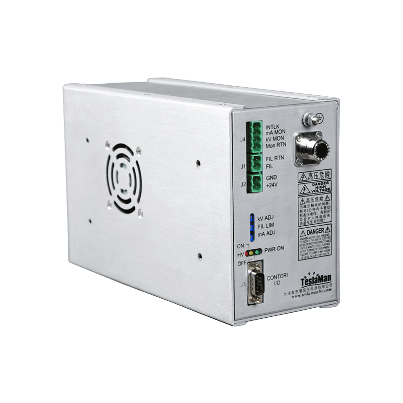
A multi-electrode partitioned power supply design is adopted, dividing the chuck into 4-8 independent electrode regions, each of which is powered by a separate power module. By real-time monitoring the leakage current of each region (accuracy 10nA), the output voltage of the corresponding module is adjusted through feedback, so that the uniformity of the electric field on the chuck surface is controlled within ±5%, avoiding local electric field concentration. At the same time, the chuck surface is coated with a 10μm-thick Al2O3 insulating coating to increase the surface breakdown voltage and delay gas ionization.
1.Optimization of Pulsed Voltage Output
Abandoning the traditional DC power supply mode, microsecond-level pulsed voltage output is adopted (pulse width 1-10μs, duty cycle 20%-50%). By reducing the average effective value of voltage, the average electric field strength of the gas in the gap is lower than the ionization threshold; at the same time, the pulse rising edge is controlled within 100ns to avoid electric field impact caused by voltage mutation. The power module has a built-in "overcurrent protection - fast shutdown" mechanism. Once a current mutation (>1μA) caused by microplasma is detected, the output can be cut off within 50ns to prevent the expansion of discharge.
3. Application Verification Effects
In the 12-inch wafer etching process, the high-voltage power supply scheme reduced the wafer surface microplasma generation rate from 15% to 0.5%, and reduced the metal impurity content (such as Fe and Cu) on the wafer surface by an order of magnitude; the line width deviation of the etched pattern was reduced from 3nm to 1nm, meeting the strict requirements of advanced processes such as 3D NAND for wafer surface quality, and the chip yield was increased by 30%.