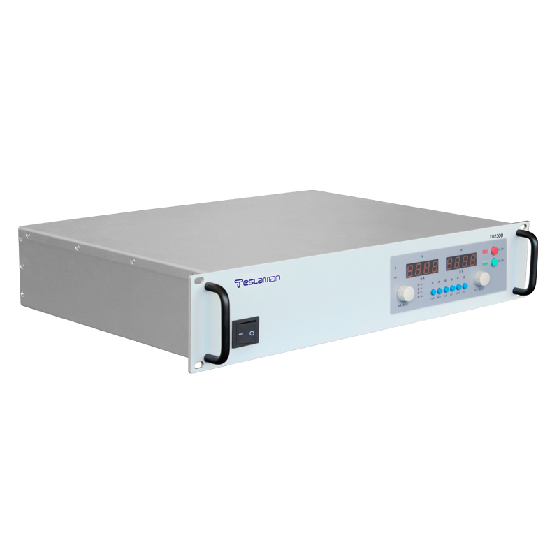
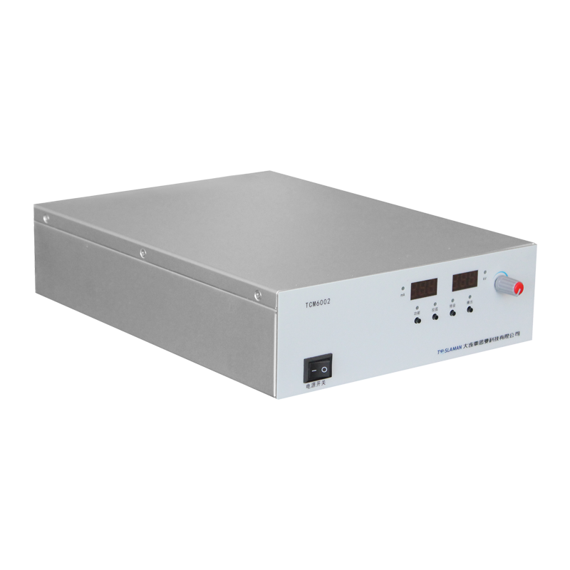
Intelligent Dielectric Loss Compensation Technology for Electrostatic Chuck High-Voltage Power Supplies and Its Applications
In key processes of semiconductor wafer manufacturing such as photolithography and dry etching, the electrostatic chuck (ESC) undertakes the core functions of precise wafer clamping and temperature control. The output stability of the high-voltage power supply directly affects the uniformity of the chuck's clamping force and wafer processing accuracy. The insulating layer of the electrostatic chuck (such as aluminum oxide and aluminum nitride) has dielectric loss, which converts part of the applied high voltage into heat energy. This not only reduces the stability of the clamping force but also may cause local overheating of the wafer, resulting in pattern transfer deviations. Therefore, intelligent dielectric loss compensation technology has become the key to improving the yield of semiconductor manufacturing.
The core logic of intelligent dielectric loss compensation lies in the closed-loop control of "real-time monitoring - dynamic modeling - precise compensation". First, a high-precision Hall current sensor (accuracy ≤0.1%) is used to real-time collect the dielectric loss current, while monitoring the temperature of the insulating layer (sampling interval ≤10ms) and the power supply output frequency, establishing a coupled mathematical model of loss current with temperature, voltage, and frequency. Second, a BP neural network algorithm is used to predict the loss trend. This algorithm can independently optimize model parameters through historical process data, controlling the prediction error of loss current within 5%. Finally, the power supply output is dynamically adjusted based on the prediction results: when voltage attenuation caused by dielectric loss is detected, the output voltage amplitude is increased through an adjustable gain amplifier, and the voltage phase is corrected simultaneously to offset the phase shift caused by loss. If the temperature of the insulating layer exceeds the threshold (e.g., 80℃), a thermal compensation mechanism is activated to reduce the power density of the power supply output, avoiding the risk of dielectric breakdown.
This technology has demonstrated significant application value in 300mm wafer manufacturing. In the photolithography process, intelligent compensation reduces the fluctuation of the electrostatic chuck's clamping force from ±5% to ±1%, controls the parallelism error between the wafer and the lithography objective lens within 0.1μm, and reduces the critical dimension variation (CD Variation) by 30%, meeting the pattern accuracy requirements of the 7nm process. In the dry etching process, the uniformity of wafer temperature is improved from ±2℃ to ±0.5℃, avoiding uneven etching rates caused by local temperature differences, and the verticality of etched patterns is increased to over 98%. In addition, this technology has process compatibility, adapting to insulating layer materials with different dielectric constants (such as SiO₂ and Si₃N₄), reducing the power supply debugging time during process switching, and improving the efficiency of production lines.