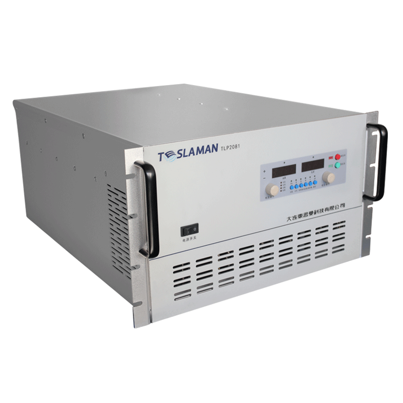
Energy-Saving Power System Upgrades for Lithography Equipment
Lithography equipment is one of the most energy-intensive subsystems in semiconductor fabrication, and its high-voltage power delivery architecture plays a central role in both operational efficiency and patterning performance. Upgrading the power system not only reduces electrical consumption but also contributes to improved thermal stability, reduced equipment downtime, and enhanced throughput. Modern energy-saving strategies require simultaneous optimization of topology, control algorithms, conversion stages, thermal design, and integration with factory-wide power management. Such enhancements must be implemented without compromising critical lithography parameters such as dose stability, illumination uniformity, focus variation, and exposure repeatability.Lithography tools rely on several high-voltage modules powering excimer lasers, light modulation units, electrostatic chucks, high-precision stages, and beam-shaping components. The excimer laser subsystem alone can account for a significant portion of total power consumption. Energy-saving upgrades begin with optimizing conversion efficiency in high-voltage laser drivers. Traditional converter topologies, while robust, often operate at suboptimal switching frequencies and suffer from conduction loss. Transitioning to wide-bandgap semiconductor switches allows much higher switching frequencies, reduced switching loss, and smaller passive components. These improvements raise efficiency while enabling faster regulation and reduced ripple.A multi-stage architecture also contributes significantly to energy optimization. Instead of using a single monolithic converter, a partitioned design divides power processing into bulk AC-DC conversion, intermediate bus stabilization, and high-precision HV regulation. Each stage is optimized for its load characteristics and conversion ratio. Bulk converters adopt soft-switching techniques to minimize losses, while the HV regulation stage employs resonant or quasi-resonant modulation to deliver clean and tightly controlled output. This separation ensures that the high-precision stage operates under consistent input conditions, improving regulation without wasting energy in over-dimensioned components.Energy recovery systems greatly enhance overall efficiency. During exposure cycles and stage movement, significant reactive energy is generated. Regenerative braking circuits in the stage module capture kinetic and electrostatic energy and feed it back into the power bus. Similarly, capacitive recovery circuits in electrostatic chuck drivers recycle charge during clamping and release cycles. These recovered energies reduce the workload on the front-end power converters, directly decreasing total power consumption.Thermal management is another major contributor to energy usage. High-voltage modules generate heat during switching and conduction, and cooling systems often consume substantial electrical power. Energy-efficient upgrades involve redesigning cooling channels, optimizing airflow geometry, and implementing liquid-based or phase-change cooling where appropriate. Advanced thermal spreading materials distribute heat more uniformly, preventing thermal hotspots that degrade electrical performance. Dynamic cooling control adjusts fan or pump speed based on predicted thermal load rather than constant operation, reducing unnecessary energy expenditure.Power factor correction (PFC) ensures that lithography tools draw power more efficiently from the factory grid. High-performance PFC circuits minimize harmonic distortion and reactive power, reducing both energy waste and electrical stress on upstream distribution networks. Optimized PFC also stabilizes the voltage delivered to sensitive lithography subsystems, contributing to dose stability and improved imaging accuracy.Electrostatic chuck systems rely on high-voltage supplies for wafer clamping. These supplies often operate continuously even when full clamping force is unnecessary. Energy-saving algorithms adjust clamping voltage dynamically based on wafer mass, temperature, and process phase. By reducing voltage during idle periods, energy consumption decreases without compromising wafer position stability. Fast-response regulators ensure immediate voltage restoration during exposure or measurement events.The illumination and optical subsystems benefit from digital-enhanced HV regulation. Light modulators, such as liquid crystal arrays or micro-mirror assemblies, require stable HV biasing. Optimizing their drivers to operate in low-loss regions of the switching cycle reduces energy use while preserving fast response. Adaptive control techniques measure optical performance indicators and adjust HV bias dynamically to maintain uniform illumination with minimal electrical overhead.Mechanical vibration in lithography stages creates additional energy loss and reduces tool accuracy. Upgraded HV drivers with smoother switching and reduced electromagnetic emission minimize interference with stage sensors and actuators. As a result, the stage consumes less correction energy to maintain position accuracy. This interaction between HV noise reduction and mechanical efficiency highlights the cross-disciplinary nature of lithography power optimization.Integration with fab-level power management is increasingly important. High-voltage supplies report real-time energy usage, thermal load, and efficiency metrics to the factory control system. Predictive algorithms identify periods of reduced lithography demand and transition the power system into low-energy standby modes. During peak activity, the system pre-warms critical components for optimal efficiency. Such coordination prevents sudden power spikes, enhances grid stability, and reduces operational cost.High-voltage component durability also contributes to energy savings. As components degrade, losses increase due to rising leakage currents, reduced switching efficiency, and higher thermal resistance. Energy-aware health monitoring detects early degradation signatures such as partial discharge activity, thermal drift, or increased ripple. Maintenance can then be scheduled proactively, preventing energy waste and minimizing downtime.Noise suppression techniques have energy implications as well. Excessive filtering increases passive losses. Instead, modern HV designs employ active noise reduction, digital ripple cancellation, and optimized magnetic components to maintain low noise at reduced loss. Component placement and circuit routing are analyzed to decrease parasitic capacitance and inductance, enhancing both power efficiency and signal integrity.Finally, modular HV architecture supports scalable energy-saving upgrades. By dividing the HV system into hot-swappable modules, older and less efficient units can be replaced incrementally without halting production. This approach allows gradual optimization and faster adoption of emerging high-efficiency technologies. Modules communicate via optical or differential digital links, maintaining noise immunity while reducing idle power consumption.Through advanced converter technology, thermal management improvements, energy recovery systems, adaptive control algorithms, and integration with fab-level energy strategies, high-voltage power upgrades significantly enhance lithography equipment efficiency. These enhancements reduce operational costs, increase system longevity, and improve process performance while meeting the strict precision requirements of semiconductor manufacturing.
