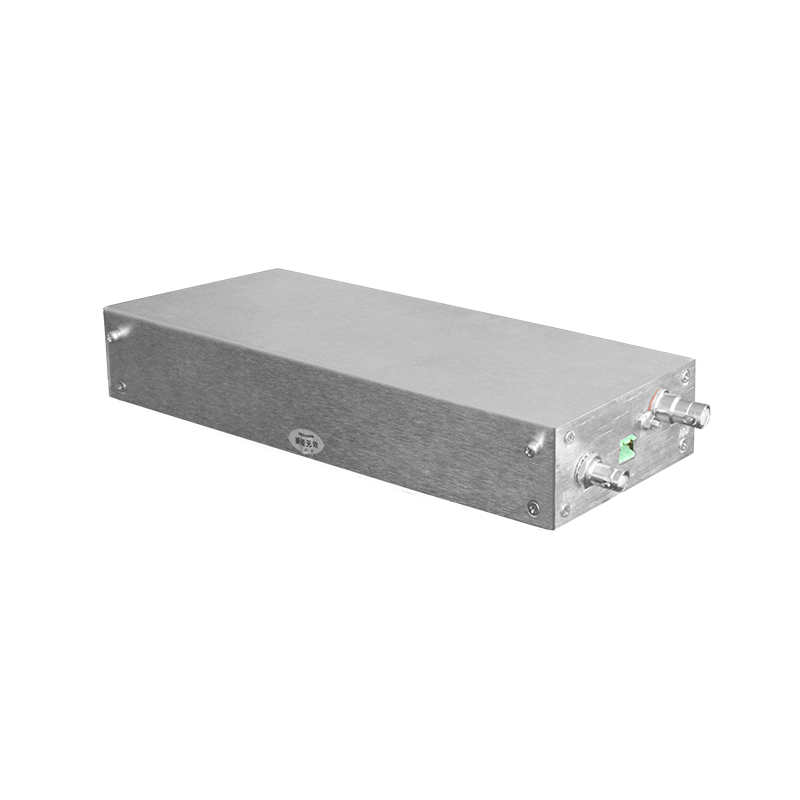
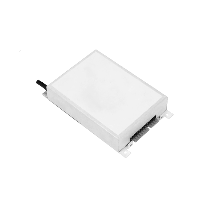
Localization and Innovative Applications of High-Voltage Power Supplies in Etching Equipment
The push toward self-reliance in semiconductor equipment has spotlighted the critical need for robust domestic alternatives in core components, particularly high-voltage power supplies used in plasma etching machines. These supplies are essential for generating the electric fields that sustain plasma discharges, controlling ion fluxes, and dictating etch selectivity and anisotropy. Developing localized versions involves not only replicating established performance benchmarks but also introducing innovations tailored to emerging process challenges, such as etching wide-bandgap materials or complex 3D architectures.
At the heart of localization efforts is the redesign of power conversion topologies to achieve high efficiency and compactness using readily available semiconductor switches. Traditional linear or resonant converters often suffer from thermal limitations at multi-kilowatt levels, but localized designs leverage wide-bandgap devices to operate at higher switching frequencies, reducing transformer sizes and improving transient response. This enables etching equipment to handle rapid pulsing regimes required for atomic layer etching, where precise control over ion energy spectra minimizes lattice damage in sensitive substrates.
Innovative applications arise from customizing waveform shaping capabilities. For example, asymmetric bipolar pulses generated by localized high-voltage modules can tailor ion energy distributions to suppress charging in high-aspect-ratio features, a persistent issue in gate-all-around transistor fabrication. By incorporating arbitrary waveform generation, these supplies allow engineers to experiment with tailored voltage profiles that enhance sidewall passivation without relying on exotic gas mixtures, broadening process windows for domestic fabs.
Another area of innovation is the integration of multi-channel outputs within a single unit. Localized supplies can simultaneously drive source plasma generation, substrate biasing, and electrostatic chucking, synchronizing phases to optimize radical-to-ion ratios. This multifunctionality reduces system complexity and footprint, a boon for cost-sensitive production lines aiming to compete globally.
In reactive ion etching of compound semiconductors, localized high-voltage systems introduce adaptive impedance matching algorithms that compensate for varying plasma loads during multi-step recipes. This ensures stable power delivery even as chemistry shifts from fluorinated to chlorinated gases, enabling seamless etching of heterogeneous stacks like those in power electronics devices.
The pursuit of localization has also driven advancements in arc management. High-voltage supplies now feature predictive arc detection using machine learning on current and voltage signatures, quenching events in microseconds to protect delicate masks. This innovation extends mask lifetime and improves yield in volume manufacturing of logic and memory chips.
For deep silicon etching, innovative pulsing strategies from localized supplies alternate high-energy bombardment with low-energy radical exposure periods, achieving smoother bottoms and reduced scalloping. Such techniques are particularly valuable in MEMS fabrication, where mechanical integrity is paramount.
Localized development emphasizes modularity and upgradability. Supplies designed with field-replaceable sub-modules allow fabs to incorporate future enhancements, such as higher voltage ratings for emerging vacuum ultraviolet excimer sources in advanced lithography-adjacent etching.
In terms of diagnostics, embedded sensors in localized high-voltage units provide real-time health monitoring, feeding data to fab-wide analytics platforms. This facilitates predictive maintenance, reducing unplanned outages that plague imported systems with proprietary lock-ins.
Innovative cooling solutions, like immersion or microfluidic channels, enable higher power densities in localized designs, supporting denser plasma sources for faster etch rates without compromising stability.
The application of high-voltage power in remote plasma sources represents another frontier. Localized supplies power upstream radical generators that decouple activation from the main chamber, allowing gentler processing of temperature-sensitive materials like organic interlayers in hybrid bonding.
For cryogenic etching processes gaining traction in quantum device fabrication, localized high-voltage systems maintain performance at reduced temperatures, with compensated drivers that counteract increased dielectric strengths.
Localization fosters collaboration between equipment makers and material scientists, leading to supplies optimized for specific domestic gas precursors or chamber geometries. This customization yields superior selectivity in etching novel materials like transition metal dichalcogenides.
In pulsed laser-assisted plasma etching hybrids, high-voltage synchronization with optical triggers opens new pathways for ultra-precise material removal, an innovative leap enabled by flexible localized controllers.
Overall, the localization of high-voltage power supplies in etching equipment transcends mere substitution, catalyzing innovations that address unique challenges in advanced node production. These developments enhance process flexibility, reduce dependency on external technologies, and position domestic capabilities at the forefront of semiconductor evolution.