High-Voltage Power Supplies Driving Precision Control in CMP
Precision control in modern chemical mechanical polishing demands electrostatic chucking systems capable of maintaining wafer-to-pad force uniformity at the single-digit newton level across 300 mm diameters while compensating for consumable wear, slurry distribution changes, and incoming wafer variability. High-voltage power systems have evolved into active participants in the closed-loop control architecture rather than passive voltage sources.
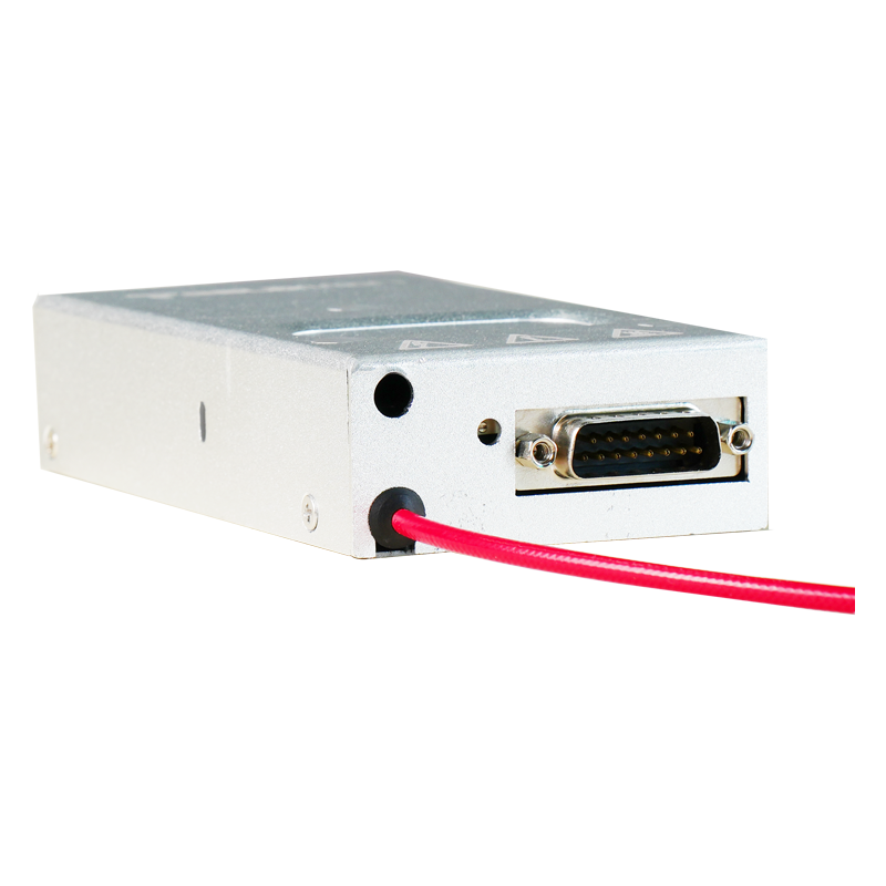
Multi-zone electrostatic chucks with twenty or more independent zones require individual high-voltage channels regulated to better than ±2 V across the full 0-2000 V range. Precision supplies achieve this through 18-bit digital-to-analog control combined with kelvin sensing directly at the chuck electrode feedthroughs, eliminating errors from cable IR drop and connector contact resistance. Real-time correction tables stored in non-volatile memory compensate for measured dielectric thickness variations between chuck refurbishments, ensuring force repeatability wafer-to-wafer even after thousands of wafers into a pad life.
Dynamic force profiling synchronized with platen rotation enables active correction of removal rate signatures. By modulating zone voltages at rotational frequency and its harmonics, the power system can induce controlled radial force gradients that counteract slurry transport effects or pad groove clogging. This closed-loop capability routinely reduces within-wafer nonuniformity from typical 4-6% with fixed voltage to under 1.5% without changing consumables.
Backside gas pressure fluctuations represent another source of force disturbance. Precision supplies incorporate high-bandwidth current monitoring at nanoampere resolution to infer instantaneous gap changes from helium ionization current. When leak rate increases due to wafer bow or seal wear alters effective dielectric constant, the controller adjusts voltage within milliseconds to restore target clamping pressure, preventing the micro-slip events that generate scratch defects.
Temperature-induced chucking force drift is compensated through embedded resistance temperature detectors in each zone coupled with physics-based models that predict dielectric constant variation. Voltage is continuously trimmed to maintain constant E-field strength, preventing over-clamping at elevated temperatures that exacerbates edge rollover while avoiding under-clamping during cold starts that risks wafer pop-off.
Active vibration damping through electrostatic force modulation has emerged as a powerful precision enhancement. Accelerometers mounted on the polishing head feed data to the power supply which applies counter-phase force perturbations at the dominant resonance frequencies, reducing vibration amplitude by up to 70%. This directly translates to lower edge exclusion and improved nanoscale planarity.
Precision de-chucking sequences prevent residual charge that causes wafer sticking or placement errors. Supplies execute multi-stage discharge with programmed current limits that follow measured capacitance decay, achieving residual voltage below 5 V in under 200 milliseconds while never exceeding field strengths that could launch particles. This capability supports transfer repeatability better than 50 μm required for direct bonding preparation processes.
Integration with optical endpoint systems allows anticipatory voltage adjustment as remaining film thickness approaches target. By gradually reducing clamping force in concert with downforce reduction, the system minimizes shear stress at interface layers, dramatically lowering delamination risk in fragile low-k and ultra-low-k stacks.
The combination of these precision control features has enabled CMP processes to achieve sub-nanometer planarity across full 300 mm wafers with incoming topography exceeding 100 nm, while simultaneously supporting removal rate stability better than ±1% over marathon qualifications exceeding 50 000 wafers per pad set.