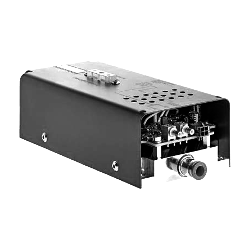
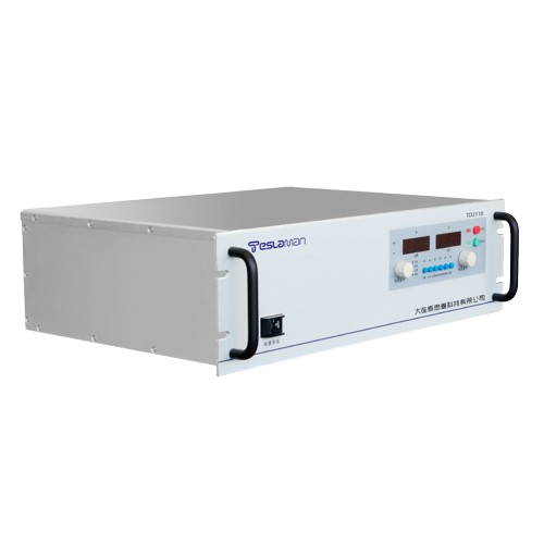
High-Voltage Power Supplies Driving Optimization of Wafer Cleaning Processes
The relentless scaling of semiconductor devices has elevated post-process residue removal to one of the most critical yield-limiting steps, where even sub-10 nm particles or atomic-layer organic contamination can render entire dies nonfunctional. High-voltage power systems have moved from peripheral components to active drivers of cleaning performance by enabling precise control over megasonic cavitation, electrostatic particle attraction/repulsion, and charge-neutralized drying environments that directly influence removal efficiency and defectivity.
Megasonic cleaning efficacy depends critically on the temporal stability and spectral purity of the acoustic energy delivered to the wafer surface. Advanced high-voltage supplies generate tightly regulated sinusoidal bursts at 800-1000 kHz with amplitude stability better than 0.3% cycle-to-cycle through resonant conversion topologies that lock output frequency to the transducer’s instantaneous mechanical resonance via real-time phase feedback. This eliminates the low-frequency amplitude modulation that previously produced uneven cavitation zones and left residue in wafer center or edge regions. By incorporating programmable envelope shaping—slow rise to avoid transient shock waves followed by constant amplitude and controlled decay—the supply minimizes silicon lattice damage while maximizing particle detachment force, routinely achieving greater than 99.5% particle removal efficiency on patterned low-k surfaces that were historically marginal.
Electrostatic-assisted cleaning leverages programmable bipolar high-voltage waveforms to create oscillating electric fields that prevent particle re-deposition during rinse steps. Supplies capable of delivering ±1200 V at slew rates exceeding 8 kV/µs generate field strengths sufficient to overcome van der Waals adhesion on hydrophobic films without inducing electrostatic discharge events. Adaptive polarity sequencing synchronized with wafer rotation ensures every azimuthal sector experiences identical field exposure, eliminating streak defects that plagued earlier fixed-polarity designs. Real-time surface potential monitoring via non-contact sensors closes a feedback loop that adjusts waveform duty and amplitude to maintain near-zero net charge throughout the cleaning sequence, dramatically reducing re-attraction of airborne molecular contaminants in FOUP mini-environments.
Marangoni drying performance receives similar enhancement through high-voltage assisted gradient control. Short-duration unipolar pulses applied during IPA vapor introduction amplify the surface tension gradient beyond what vapor concentration alone can achieve, accelerating meniscus withdrawal and reducing drying time by 35-45%. The required kilovolt pulses with precisely controlled energy content demand supplies incorporating gallium nitride output stages that maintain sub-microsecond edge fidelity without ringing that could launch droplets back onto the wafer.
Ozone-based cleaning processes benefit from high-voltage corona discharge modules integrated into the same power chassis. By synchronizing ozone generation pulses with megasonic off-periods, the supply maximizes dissolved ozone concentration exactly when acoustic streaming is absent, optimizing organic strip rate while minimizing quartz rod erosion from simultaneous exposure to high-intensity ultrasound and reactive species.
Energy-based process control has replaced time-based recipes entirely. Supplies continuously integrate delivered acoustic power and compare against calibrated removal models stored in non-volatile memory, terminating megasonic exposure the instant target dose is reached regardless of transducer aging or temperature drift. This eliminates over-processing that previously contributed to surface roughening on delicate high-k metal gate stacks.
Charge damage mitigation during bevel cleaning represents another optimization frontier. Dedicated high-voltage channels apply localized fields only to the wafer extreme edge while shielding the active die area through grounded guard rings, enabling aggressive polymer removal at the bevel without risk to thin gate oxides.
The cumulative effect of these high-voltage driven optimizations is a reduction of total cleaning time by 25-40% while simultaneously improving particle performance by one to two orders of magnitude and achieving electrostatic defect densities below detectable limits in advanced 3D NAND and logic devices carrying features smaller than 5 nm.