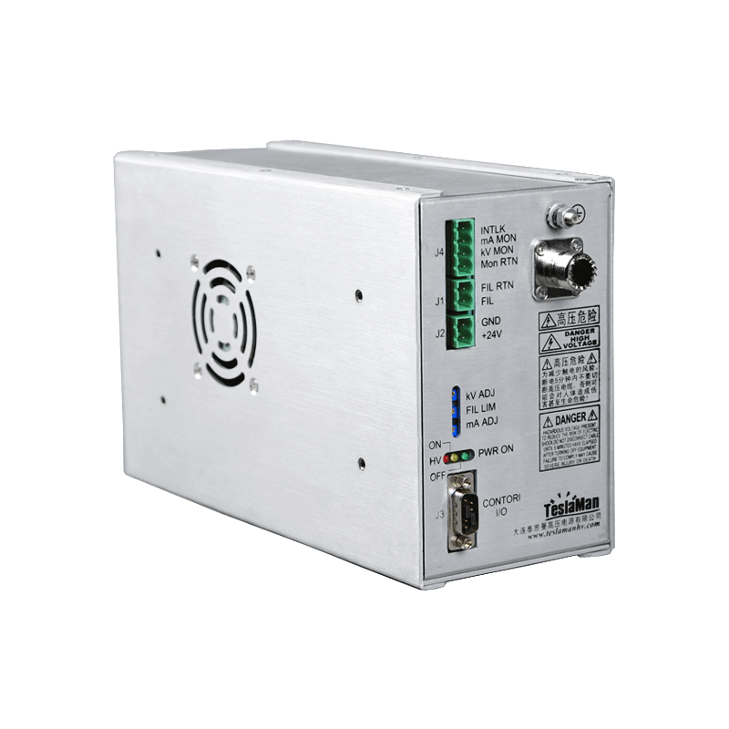
High-Voltage Power Supplies Enhancing Efficiency and Precision in Cleaning Production Lines
Precision and efficiency in modern wafer cleaning lines are increasingly limited by the dynamic performance of high-voltage power delivery systems that drive megasonic transducers and electrostatic charge management functions. Contemporary supplies achieve simultaneous gains through ultrafast response times, adaptive energy dosing, and closed-loop stability maintenance that translate directly into higher wafer throughput and lower defectivity.
Megasonic precision begins with output voltage regulation better than ±0.5 V across the entire 400-1200 V operating range during high-power bursts. This requires 20-bit effective resolution in the control loop combined with predictive gate drive that compensates for power stage delay variations caused by temperature and aging. The resulting amplitude stability eliminates the low-frequency beating that previously produced microscopic cavitation shadows responsible for sub-20 nm particle retention in pattern-dense areas.
Energy dosing accuracy replaces crude time-based control with coulometric integration of actual acoustic power delivered to the wafer surface. Supplies continuously measure forward and reflected power at microsecond intervals while applying real-time phase correction to maintain greater than 98 % transfer efficiency. When integrated power reaches the exact dose required for the specific incoming contamination level—determined by upstream metrology feedback—the burst terminates within one acoustic cycle, eliminating over-exposure that contributes to surface micro-roughness on delicate III-V materials and low-k dielectrics.
Transient response during burst initiation represents another precision frontier. Supplies now achieve full amplitude within three electrical cycles through pre-charged resonant tanks and predictive rail boosting that anticipates the sudden load presented by piezoelectric transducers. This eliminates the gradual ramp-up periods that previously forced conservative overlap between chemistry dispense and acoustic activation, allowing 15-20 % reduction in total chemistry consumption while improving residue removal through better temporal alignment of physical and chemical cleaning mechanisms.
Charge control precision reaches sub-50 V surface potential uniformity across 300 mm wafers through independent regulation of positive and negative ion currents based on real-time feedback from multiple non-contact sensors positioned around the drying module. Adaptive algorithms compensate for electrode aging and airflow variations, maintaining neutralization time stability better than ±8 % over 10 000 wafer cycles without manual adjustment.
Efficiency gains compound through burst-mode operation that completely disables all power stages between cleaning events. Gallium nitride primary switches and silicon carbide synchronous rectifiers enable transition from zero to full 3 kW output in under 120 microseconds while achieving greater than 95 % overall efficiency during the active portion of the duty cycle. When combined with predictive pre-staging triggered by wafer scheduling data, this eliminates the continuous standby losses that previously accounted for 30-40 % of total energy consumption in low-utilization periods.
Multi-transducer systems benefit from phase-coherent operation across all quartz rods. Master-slave clock distribution with picosecond jitter maintains fixed relative phase relationships that prevent destructive interference zones, achieving greater than 99 % cavitation uniformity measured via high-speed foil erosion testing. This directly translates to lower particle adders in high-aspect-ratio memory structures where even minor acoustic shadowing can leave fatal residue.
Watermark prevention during final rinse leverages precisely timed electrostatic repulsion pulses that activate only during the critical spin-speed transition where liquid films are thinnest. The required kilovolt rectangular waveforms with nanosecond edges demand supplies incorporating distributed output switching directly at the chamber feedthrough, eliminating cable-induced ringing that previously limited pulse fidelity.
The net impact across production lines running advanced logic and DRAM processes shows 25-35 % higher wafer throughput through reduced process step times combined with defect density improvements exceeding one order of magnitude for particles larger than 12 nm, demonstrating that high-voltage subsystem performance remains a primary lever for cleaning line optimization.