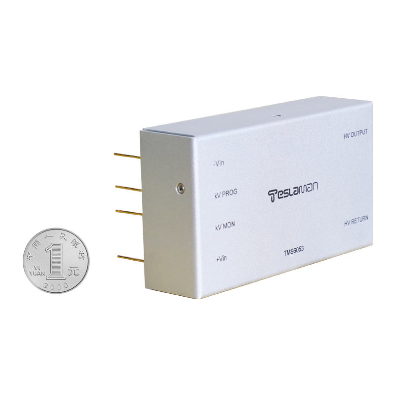
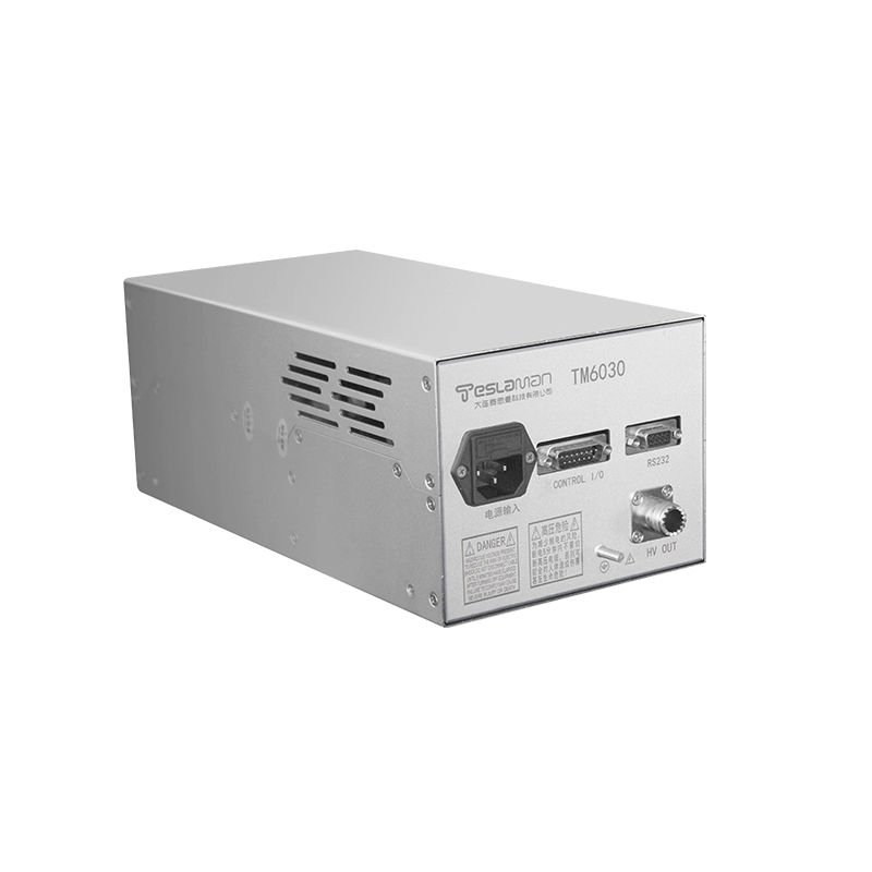
Bipolar Bias High-Voltage Power Supply for 320 kV Ion Implantation Systems
High-energy ion implanters operating at terminal voltages up to 320 kV increasingly require wafer bias capability from –25 kV to +20 kV to control secondary electron emission, suppress charging of thick photoresist, and enable precise energy contamination filtering. Dual-polarity bias supplies must therefore deliver smooth transitions through zero volts in under 8 ms while maintaining regulation better than ±8 V during 3 mA load steps typical of phosphorus and boron beams.
The topology uses a full H-bridge of 30 kV-rated insulated-gate bipolar transistors driving a 1:20 air-core step-up transformer followed by a single-stage voltage doubler/tripler selectable via solid-state relays. Positive and negative outputs share the same secondary winding through center-tapped rectification, eliminating the discontinuity at zero crossing that plagued earlier dual-rectifier designs. Transition through zero is achieved by ramping the primary modulation index from +100 % to –100 % in a single continuous sine wave, resulting in 6.4 ms zero-crossing time with less than 12 V overshoot.
Regulation during large load transients is maintained by a hybrid analog-digital control loop: a 180 kHz analog proportional-integral stage handles fast transients, while a slower digital loop updates reference offsets every 200 µs to null steady-state error from transformer magnetizing current and diode forward drop variation. Beam-induced load steps from 0 to 2.8 mA cause less than 14 V excursion with 1.8 ms settling to ±5 V.
Charge-balance control prevents net DC current into the platen insulator stack. Integrated coulombmeters on both polarities track total transferred charge in each direction; when imbalance exceeds 8 µC (corresponding to 18 V surface potential on a 15 kΩ·cm wafer), the supply injects automatic compensation pulses of opposite polarity during beam-off periods, maintaining wafer potential within ±4 V over full cassette processing.
Arc protection uses a two-threshold system: fast analog detection at 18 A collapses output in 1.2 µs via primary bridge disable, while a slower digital monitor evaluates arc energy and inserts extended dead-time for events exceeding 2 mJ to allow insulator surface recovery. Recovery ramp rate is automatically reduced after multiple arcs in the same wafer to prevent repetitive stress that previously caused dielectric tracking.
Thermal management employs oil-free forced-air cooling with variable-speed blowers referenced to IGBT junction temperature sensors, maintaining case temperature within ±2.5 °C across ambient swings from 18 °C to 32 °C common in implant bays. This eliminates oil leakage risks and reduces acoustic noise below 58 dB(A) during low-duty operation.
These bipolar bias supplies routinely achieve dose uniformity improvements of 38 % on 60 µm thick photoresist patterns by suppressing charging-induced beam deflection, while enabling energy purity better than 1 part in 10⁶ through precise deceleration lens control during high-energy arsenic implants.
