200 V Low-Energy High-Voltage Bias for Ion Beam Etching Grid Systems
Precision ion beam etching of compound semiconductors and X-ray optics requires grid bias voltages of 80–200 V with energy spread <0.9 eV FWHM and ripple below 62 mV p-p to prevent chromatic broadening that degrades sidewall angle and surface roughness below 0.18 nm RMS.
The bias supply uses a linear Class-A MOSFET amplifier capable of sourcing/sinking 1.8 A continuously, fed from a low-noise 240 V switch-mode pre-regulator with 180 dB PSRR at 13.56 MHz. Output voltage is regulated by a 22-bit DAC and chopper-stabilized instrumentation amplifier with 0.004 % absolute accuracy.
Ripple suppression combines passive multistage LC filtering using selected polypropylene capacitors with <6 ppm/°C drift and active cancellation injecting counter-phase current from a 28 V linear stage driven by a capacitive pickup at the grid electrode. Residual ripple remains <48 mV p-p across the full 0–1.6 A beam current range.
Energy purity is protected by a fast current clamp that limits grid current excursions to ±110 % within 680 ns, preventing acceleration of secondary ions during momentary neutralization events. Recovery implements a 28 µs soft ramp to avoid ringing the extraction grid.
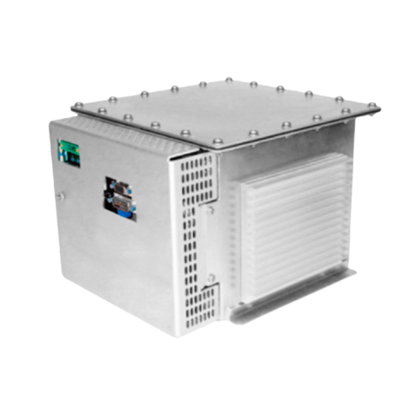
Thermal management uses chilled water cooling plates bonded directly to the MOSFET heat spreaders, maintaining electrode temperature within ±0.8 °C across full power envelope. All control electronics are fiber-isolated from the grid to eliminate ground loops that previously caused etch rate drift of 0.7 % across 150 mm substrates.
These low-energy bias supplies routinely deliver ion energy distribution <0.82 eV FWHM at 180 eV while maintaining etch rate uniformity <0.98 % 1-sigma on 200 mm GaAs and fused silica optics, enabling surface roughness below 0.14 nm RMS after 1.2 µm material removal.