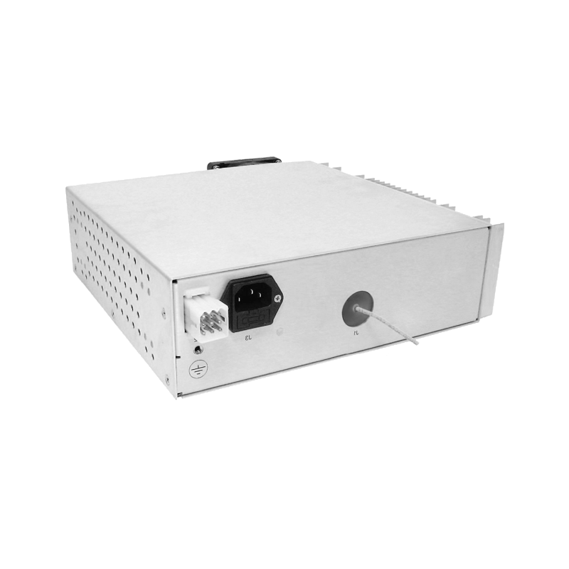
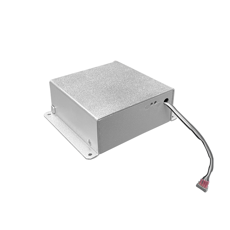
Electron beam exposure high voltage power supply graphic writing accuracy
In the realm of advanced nanofabrication, electron beam lithography (EBL) stands as a pivotal technique for defining patterns with features well below the diffraction limit of light. The precision of this direct-write process, however, is inextricably linked to the performance of its high-voltage power supply, which accelerates the electron beam. The relationship between high-voltage stability and pattern placement accuracy, line-edge roughness, and critical dimension uniformity is profound and non-linear, demanding a power supply that transcends the specifications of conventional high-voltage modules.
The core function of the high-voltage supply in an EBL system is to establish and maintain a constant electrostatic potential, typically ranging from tens to hundreds of kilovolts, between the cathode and the anode. This potential defines the kinetic energy of the electrons. Any fluctuation in this voltage, ΔV, directly translates into a change in electron velocity and, consequently, a shift in the deflection sensitivity of the beam steering system. For a magnetic deflection system, the beam deflection is inversely proportional to the beam velocity. Therefore, a voltage ripple or drift causes a proportional positional error on the substrate. In a system writing 10 nm features, a voltage stability requirement is often in the range of 1-10 PPM over short-term (exposure of a single feature) and long-term (full-wafer write time) intervals. This necessitates a combination of ultra-stable reference sources, low-drift feedback networks, and architectures immune to environmental perturbations.
The architecture of such a supply is meticulously engineered. A high-frequency, resonant switching inverter generates the basic high voltage from a low-voltage DC source. This topology is chosen for its inherent efficiency and reduced stress on switching components, which minimizes a source of long-term parameter drift. The generated high voltage is then meticulously filtered through a multi-section, oil-immersed or gas-insulated RC and LC ladder network. This passive filter is designed not just for attenuation but for a predictable phase response, ensuring stability when closed within a global feedback loop. The heart of the stability lies in the feedback sensing network. A high-value, low-temperature-coefficient resistor divider, often consisting of precision wire-wound or bulk-metal foil resistors housed in a temperature-controlled oil bath, scales the output voltage down to a metrology level. This scaled voltage is compared against an ultra-stable reference, such as a Josephson junction array standard or a specially aged and oven-controlled Zener diode, using a null-detector amplifier with femtoampere input bias currents.
The challenge of load regulation is particularly acute. The electron beam current, while small (picoamps to microamps), can be modulated at high frequencies as the beam blanks on and off. Each transition represents a step change in load. The power supply must exhibit exceptionally low output impedance across a frequency spectrum from DC to several megahertz to prevent these load transients from causing voltage sags or spikes that would distort the exposure dose at pattern edges. This is achieved through a combination of wide-bandwidth error amplification, local decoupling using high-voltage, low-inductance capacitors placed physically close to the beam column connection, and sometimes, predictive feed-forward compensation based on the blanking signal.
Environmental immunity is a parallel battle. Changes in atmospheric pressure and humidity alter the breakdown characteristics and corona inception voltage within the system, potentially introducing subtle leakage current paths that affect the feedback divider ratio. The high-voltage enclosure is thus sealed and filled with a dielectric gas like sulfur hexafluoride (SF6) or nitrogen at controlled pressure. Temperature gradients are perhaps the most pernicious influence. Every component in the chain—resistors, references, amplifiers—has a temperature coefficient. Active temperature stabilization of the entire high-voltage generator and sensing module is standard. Furthermore, thermal design ensures that heat from lossy components like series-pass tubes or switching devices is dissipated in a manner that does not create dynamic thermal gradients across critical sensing elements.
The final measure of performance is not on the power supply's output terminals, but on the exposed wafer. Metrology tools like critical-dimension scanning electron microscopes (CD-SEM) and laser interferometric stage systems are used to correlate pattern placement errors with power supply monitoring data. Techniques such as "write-and-read" tests, where a periodic grating is written and its period precisely measured, allow for the extraction of the beam's deflection sensitivity coefficient and its variation over time. This system-level calibration data is often fed back into the pattern generator to apply software-based corrections, but the foundational limitation remains the intrinsic stability of the high-voltage field that propels and defines the electron beam's influence. Thus, the high-voltage power supply is not merely a utility in an EBL tool; it is the bedrock upon which nanometric patterning fidelity is built.