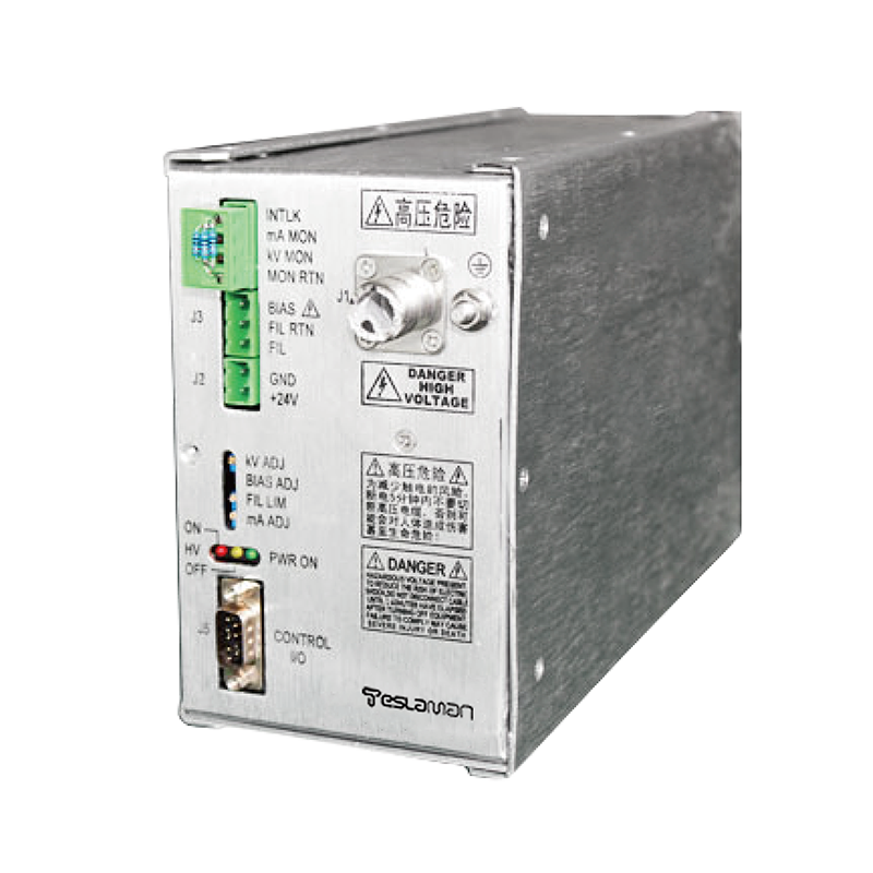
Research on Bipolar Adsorption Power Supply of Electrostatic Chuck
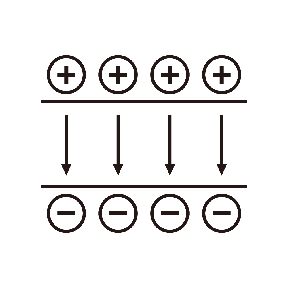
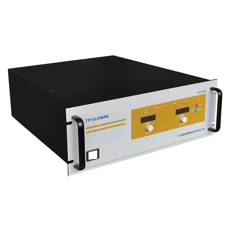
The electrostatic chuck (ESC) has become the dominant substrate clamping technology in semiconductor plasma processing equipment, enabling precise thermal management and minimal particulate contamination. The evolution of process complexity, particularly with the advent of radio-frequency (RF) driven plasmas for etching and chemical vapor deposition, has driven the need for advanced electrostatic clamping power supplies capable of bipolar operation. Unlike traditional unipolar or DC chucks, a bipolar ESC utilizes two independent interdigitated electrode sets embedded within the dielectric chuck surface. A bipolar power supply applies equal-magnitude but opposite-polarity potentials to these electrode sets, creating a strong electrostatic holding force on the wafer while presenting a net-zero DC potential to the wafer substrate. This research delves into the critical requirements and technological implementations of such bipolar high-voltage supplies.
The primary impetus for bipolar ESC adoption is the mitigation of plasma charging damage. In a unipolar chuck, the wafer rests on a dielectric layer atop a single biased electrode. During RF plasma exposure, charge accumulation on non-conductive layers can occur, leading to unpredictable potential differences and potentially damaging gate oxides in sensitive devices. The bipolar configuration, by maintaining the wafer at a virtual DC ground relative to the two opposing fields, drastically reduces this net charging effect. This places an immense burden on the power supply's symmetry and dynamic response. The two output channels (+HV and -HV) must be precisely balanced in magnitude, typically to within 0.1% or better, to ensure the wafer's floating potential remains truly near zero. Any imbalance directly translates into a net DC bias on the wafer, inviting plasma charging issues.
The architecture of a high-performance bipolar ESC supply is inherently dual-channel with master-slave or common-reference tracking. A central control system generates a voltage demand signal. This signal is simultaneously sent to a positive high-voltage module and a negative high-voltage module. The key is not independent regulation, but forced tracking. The feedback for the master channel (often the positive) controls its output directly. The slave channel's feedback loop, however, compares its own output not only to the demand signal but also to the inverted output of the master channel via a differential error amplifier. This forces the negative output to mirror the positive output in real-time, compensating for any differences in load current, component tolerances, or transient response between the two chains.
The load presented by an ESC is highly non-trivial. It is fundamentally a capacitive load, comprising the capacitance between the electrodes and the wafer, which can range from tens to hundreds of nanofarads. However, this is not a pure capacitor. The dielectric layer (often aluminum oxide or aluminum nitride) exhibits leakage, modeled as a parallel resistance. Furthermore, during a plasma process, the plasma itself forms a conductive, time-varying path to ground, effectively altering the load impedance dynamically. The power supply must be capable of sourcing and sinking current to charge and discharge this large capacitance rapidly during wafer clamping and declamping sequences, yet maintain exquisite stability during the process hold. This necessitates a design with high slew-rate capability and robust stability margins when driving a highly capacitive load, often employing output stages with high linearity and low output impedance.
A paramount consideration is fault tolerance and arc management. In the event of a wafer break or a micro-particulate inducing a localized dielectric breakdown, a direct short can occur between an electrode and the plasma or the chuck body. The power supply must detect this arc within microseconds and safely shut down the affected channel without causing a voltage overshoot on the complementary channel that could exacerbate the damage. Advanced designs incorporate fast analog arc detection circuits monitoring the rate-of-change of current (dI/dt) and optical sensors, coupled with solid-state switches that can isolate the output in less than 10 microseconds. After a fault, a controlled, low-current recovery sequence is initiated to test the integrity of the dielectric before re-applying full voltage.
Integration with the broader tool system is critical. The ESC supply receives commands from the equipment controller for clamping voltage level (which controls holding force, typically 500-5000V), and for the timing of the clamping/declamping sequence. It must also communicate status, fault conditions, and real-time voltage/current readings. In modern systems, this is done via a high-speed digital fieldbus. Additionally, the supply must be immune to the very harsh electromagnetic environment of a plasma chamber. Intense RF power, at frequencies of 13.56 MHz, 27 MHz, or 60 MHz, is coupled into the chamber, inducing common-mode and differential-mode noise on all connected cables. The ESC supply, its control electronics, and the wiring to the chuck must employ extreme levels of filtering, shielding, and galvanic isolation. The high-voltage outputs are often filtered with RF chokes and bypass capacitors tuned to the specific process frequencies to prevent the RF from leaking back into the supply or modulating the DC clamping field. Research in bipolar ESC power supplies, therefore, sits at the intersection of high-voltage engineering, precision analog control, ultra-fast protection circuitry, and electromagnetic compatibility, all in service of enabling the next generation of plasma-based nanofabrication.
