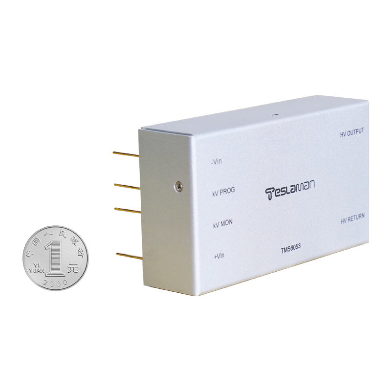
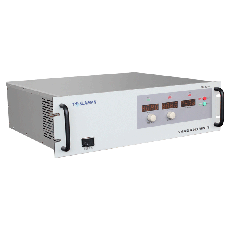
Vacuum Coating Substrate Bias Power Supply Research
The application of a controlled electrical potential to a substrate during physical vapor deposition (PVD) processes, known as substrate biasing, is a powerful technique for engineering thin film microstructure, adhesion, and stress. Moving beyond simple DC biasing, contemporary research and advanced application focus on sophisticated power supply architectures that deliver precisely shaped voltage waveforms at frequencies ranging from DC to radio frequency (RF) and into the pulsed regimes. The investigation of these substrate bias power supplies is driven by the need for independent control over the energy and flux of ions bombarding the growing film, parameters that fundamentally dictate its final properties.
The most basic function of a substrate bias supply is to attract ions from the plasma towards the substrate, imparting them with kinetic energy. In a simple DC diode configuration, a negative DC voltage applied to the substrate creates a sheath potential that accelerates positively charged ions. However, this approach has severe limitations. It is ineffective in insulating or coating insulating surfaces, as charge buildup rapidly negates the field. It also provides no independent control over ion energy and flux; both are coupled to the plasma density and the applied voltage. This has spurred research into RF biasing, where a sinusoidal RF voltage, typically at 13.56 MHz, is applied through an impedance matching network. Due to the mobility difference between electrons and ions, a negative DC self-bias voltage naturally develops on the substrate, attracting ions. The research challenge here lies in decoupling the ion energy from the ion flux. The time-averaged ion energy is related to the self-bias voltage, which is influenced by the RF power and pressure, while the ion flux is tied to the plasma density. Advanced RF bias supplies with sophisticated matching networks and precise power control allow for some tuning, but the fundamental coupling remains a constraint.
This drive for decoupled control is a primary motivator for research into pulsed and hybrid bias schemes. A pulsed DC bias supply applies a negative high-voltage pulse to the substrate. During the pulse "on" time, ions are accelerated to the substrate with an energy broadly defined by the pulse voltage. During the pulse "off" time, the plasma can flood the substrate region, neutralizing charge and allowing for cooling. By independently varying the pulse voltage (controlling ion energy), pulse width (affecting the duty cycle of bombardment), and frequency, a greater degree of separation between energy and flux parameters is achieved. Research explores the effects of these parameters on film densification, elimination of columnar growth voids, and the reduction of intrinsic stress. For example, a high voltage with a low duty cycle may deliver high-energy ions for sub-surface implantation and densification without causing excessive heating or defect generation.
The frontier of research extends into complex, non-sinusoidal waveforms and synchronized biasing. In processes like High Power Impulse Magnetron Sputtering (HiPIMS), the plasma itself is a pulsed, ultra-dense source of ions. Research focuses on bias supplies that can synchronize their output pulses with the HiPIMS pulse. A common strategy is to apply the substrate bias pulse with a specific time delay after the HiPIMS pulse, allowing the system to selectively attract the highly ionized metal species that arrive later in the pulse while ignoring the initial neutral flux. This enables unprecedented control over film texture and morphology. Other research explores the use of superimposed waveforms, such as a DC offset with an RF component, or tailored very-high-frequency (VHF) biases to manipulate the ion energy distribution function (IEDF), moving beyond a single average energy to a designed energy spectrum.
From a power supply engineering perspective, this research imposes demanding requirements. Supplies must be capable of generating high-voltage pulses with fast rise and fall times (often in the microsecond range) into a capacitive load (the substrate and its holder) without destructive ringing. They must offer precise and repeatable control over waveform parameters and synchronization with external triggers. For insulating films, the supplies must incorporate advanced arc management and charge compensation mechanisms. Furthermore, the interaction between the bias supply and the main plasma source supply is a critical area of study, as one can influence the plasma potential and thus the effectiveness of the other. Research in substrate bias power supplies is, therefore, a multidisciplinary endeavor intersecting plasma physics, materials science, and high-power electronics. Its goal is to transform the substrate electrode from a passive holder into an active, intelligent tool for atomic-scale engineering, enabling the synthesis of thin films with tailored properties for the most demanding tribological, optical, and electronic applications.