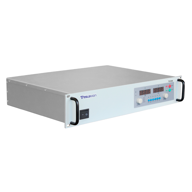
Coating Pulse Power Supply Negative Bias Cleaning Function
In advanced physical vapor deposition (PVD) processes, particularly those utilizing high-power pulsed magnetron sputtering (HPPMS) or cathodic arc deposition, the management of chamber conditioning and parasitic coating is a critical operational challenge. These high-ion-density processes excel at producing dense, adherent films but inevitably lead to the deposition of material not only on the substrate but also on chamber walls, shields, and fixtures. Over time, these insulating or semi-conducting coatings accumulate, posing severe risks to process stability. They can cause arcing, generate particulate contamination, and alter plasma impedance, leading to drifts in film properties. The integration of a dedicated negative bias cleaning function into the pulse power supply system addresses this issue proactively, enabling in-situ chamber maintenance without breaking vacuum.
The core principle of this function is fundamentally different from the substrate biasing used for film growth. A substrate bias, typically a continuous or pulsed negative DC voltage, is applied to the sample holder to control ion bombardment energy during deposition, influencing film density and stress. The cleaning bias, in contrast, is applied to specific chamber components *themselves*—often a dedicated set of electrodes, movable shutters, or even sections of the chamber wall—that are normally grounded during the main deposition phase. Periodically, these surfaces are switched to become cathodes by connecting them to a specialized high-voltage, pulsed negative output from the power supply system.
The electrical requirements for effective cleaning are distinct and demanding. The voltage must be sufficiently high (often in the range of -500V to -2000V or more) to create a strong electric field across the deposited layer, initiating a controlled discharge. The power supply must deliver this in short, high-current pulses (microsecond to millisecond width) to aggressively sputter the coating material without causing thermal overload or transitioning into a destructive, uncontrolled arc. This necessitates a power stage with very fast rise and fall times and exceptionally robust arc handling capabilities. The cleaning supply incorporates ultra-fast analog arc detection circuits that monitor the derivative of the output current (dI/dt). Upon detecting the nanosecond-scale current rise characteristic of an arc inception, the supply can shut down the output within a few microseconds and often applies a brief positive voltage pulse to quench the plasma and clear the fault condition.
The physical cleaning mechanism involves a combination of physical sputtering and, when reactive gases are introduced, chemical assistance. With a pure argon atmosphere, the high negative bias attracts argon ions which bombard the coated surface, physically ejecting atoms of the deposited material. For tenacious oxides or nitrides, introducing a small flow of oxygen or a fluorine-based gas like CF4 can create reactive species in the plasma that chemically assist in breaking down the coating, making it more volatile or easier to sputter. The cleaning process is often enhanced by rotating or rastering the cleaning electrodes to ensure uniform coverage or by using multiple electrode sets powered in a sequence.
System integration is key to this function's utility. The cleaning power supply is not a standalone unit but a tightly integrated module within the larger deposition power and control system. It shares the main DC link and control platform with the magnetron pulse generators and the substrate bias supply. The process recipe programmed into the equipment's main controller includes cleaning cycles. These are typically executed between deposition runs or after a predetermined number of cycles. The sequence is automated: the main deposition process concludes, the chamber is purged with argon, the substrate bias is disabled, and the cleaning electrodes are electrically isolated and then connected to the cleaning supply. The cleaning supply then executes a pre-programmed sequence of pulses for a set duration. During this time, the plasma is contained near the cleaning electrodes, minimizing re-deposition elsewhere. After completion, the electrodes are grounded again, and the chamber is ready for the next production cycle.
The benefits are multifaceted. It dramatically extends the mean time between manual chamber cleans, reducing downtime, consumable costs (for replacement shields), and exposure of the chamber to atmosphere. More importantly, it maintains a consistent chamber wall condition, which is critical for plasma impedance and process repeatability. This leads to improved wafer-to-wafer and lot-to-lot consistency in film properties such as thickness, stress, and composition. The negative bias cleaning function thus transforms the power supply from a mere energy delivery device into an active participant in process health management, enabling the stable, high-volume utilization of advanced pulsed PVD technologies in semiconductor, optical coating, and tooling applications.