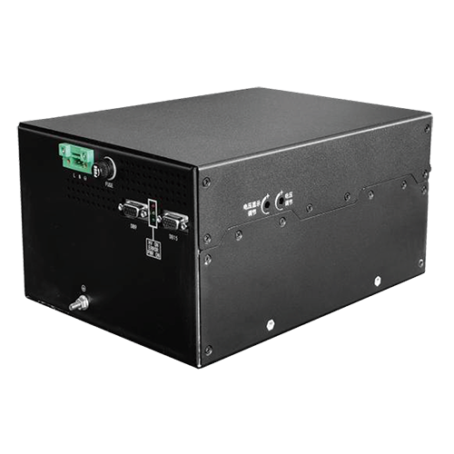
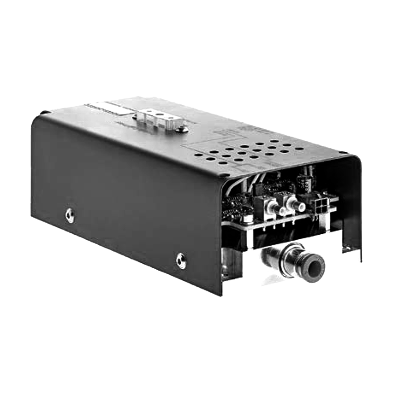
Electrostatic Chuck RF Coupled High Voltage Power Supply
In advanced plasma processing, particularly for semiconductor etching and chemical vapor deposition, electrostatic chucks (ESCs) are universally employed to clamp wafers with high force and precise temperature control. For processes involving RF plasmas, a significant challenge arises: the RF power used to generate the plasma must be coupled to the process chamber, often through the same wafer platen that serves as the ESC electrode. This creates a complex interplay between the high-voltage DC clamping potential and the high-frequency RF bias or source power. The power supply system that generates the DC clamping voltage must therefore be specifically designed to operate in this electrically hostile, coupled environment without degrading RF performance or compromising clamping stability and safety.
The primary function of the ESC DC power supply is to apply a high voltage (typically +/1000 V to +/-3000 V) to one or more electrodes embedded in the chuck ceramic. This creates an electrostatic field that polarizes the wafer (or a dielectric layer beneath it), generating a clamping force. In an RF system, this DC electrode is physically in the path of the RF current. If not properly isolated, the RF would couple directly into the sensitive DC supply, damaging it and causing unstable clamping. The solution is an "RF choke" or isolation network, but its implementation is a core part of the power supply's design philosophy.
The most common and effective method is to integrate a high-power, high-frequency inductor (the RF choke) in series with the DC output line, very close to the chuck feedthrough. This inductor presents a high impedance at the RF frequency (e.g., 13.56 MHz or 40.68 MHz), blocking the RF from traveling back to the power supply. Conversely, it presents a low impedance to the DC, allowing the clamping voltage to pass with minimal drop. The design of this choke is critical. It must handle the full DC voltage without breaking down, carry the possible DC leakage current of the chuck, and withstand the thermal load from the RF currents induced on its conductors. Its self-resonant frequency must be carefully managed to ensure it remains inductive across the entire spectrum of RF harmonics and plasma transients.
The DC power supply itself must be resilient to any residual RF that passes the choke. Its output stage is therefore heavily filtered with low-pass networks that attenuate RF frequencies by 60 dB or more. This often involves a combination of feedthrough capacitors and planar filtering within the supply's output module. The feedback path used for voltage regulation must also be filtered to prevent RF from corrupting the measurement signal, which would cause the supply's control loop to oscillate at the RF frequency. Optical isolation of control signals is frequently employed to break ground loops that could conduct RF noise.
The nature of the RF coupling dictates specific supply requirements. In a capacitively coupled plasma (CCP) system, the ESC often serves as the RF-powered electrode (the cathode). Here, a large RF voltage swing (hundreds to thousands of volts peak-to-peak) is superimposed on the DC clamping potential. The DC supply must sink or source the DC component of the ion current collected by the wafer, which now includes a rectified RF current. This requires the supply to have a fast enough response to maintain a stable DC level despite this noisy current load, acting as a stiff voltage source. In systems with a separate RF bias, the DC supply may be referenced to a large RF voltage on the chuck body, necessitating careful attention to the common-mode voltage rating of the supply's isolation.
Modern ESCs often feature multi-zone clamping for improved thermal uniformity or backside gas pressure control. This requires a multi-channel high-voltage DC supply. Each channel must have its own independent RF isolation and filtering, as the RF potentials on different zones may not be identical. Cross-talk between channels must be minimized. Furthermore, advanced chucking algorithms may involve dynamically adjusting zone voltages during the process to manage wafer temperature or stress, requiring these multi-channel supplies to have programmable, synchronized output capability.
Safety systems are paramount due to the combination of high DC voltage and high RF power. The DC supply must have a very fast (<1 ms) discharge circuit to safely de-chuck the wafer when the process is complete or in an emergency. This discharge path must also be designed to handle RF. Interlocks must ensure that the high DC voltage cannot be applied if the RF matching network is in a fault state or if the chamber is not under vacuum. The supply must also include continuous monitoring of chuck leakage current. A sudden increase in leakage can indicate a crack in the chuck ceramic or a plasma penetration event, requiring an immediate shutdown to prevent arcing and wafer damage.
In summary, an RF-coupled electrostatic chuck high-voltage power supply is a hybrid device, merging high-voltage DC engineering with RF power integrity management. Its design is dominated by the need for impervious RF isolation via integrated chokes and filtering, stability in the presence of RF-modulated plasma loads, and robust safety for operation in an environment where kilowatts of RF and kilovolts of DC coexist. Its reliable performance ensures stable wafer clamping, which is the foundation for precise temperature control and consistent process results in the manufacture of advanced logic and memory devices.