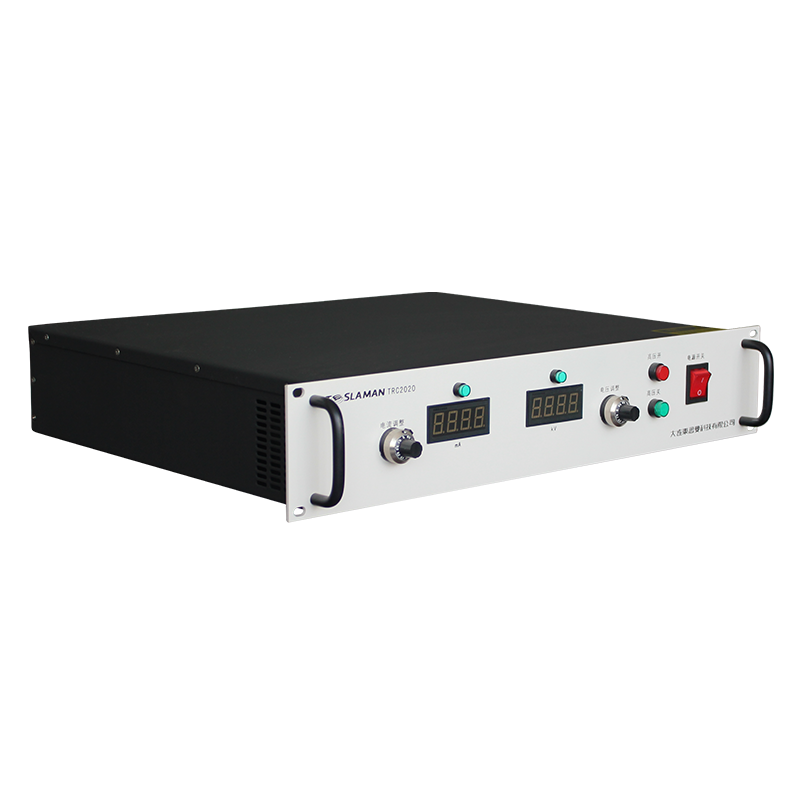
Focused Ion Beam Nanofabrication High Voltage Scanning Power Supply
Focused Ion Beam (FIB) systems have evolved from mere imaging and cross-sectioning tools into sophisticated nanofabrication platforms capable of direct-write milling, ion-induced deposition, and even nanoscale patterning with sub-10 nm resolution. At the core of this capability is the electrostatic or electromagnetic beam deflection system, which directs the focused gallium or helium ion beam across the workpiece with extreme precision. The high-voltage power supplies that drive the scanning electrodes are not merely voltage sources; they are the critical actuators that translate digital pattern data into physical, atomic-scale removal or addition. Their performance in terms of stability, speed, linearity, and dynamic response directly defines the FIB's patterning fidelity, edge acuity, and throughput.
The scanning subsystem typically requires two independent, high-voltage, bipolar outputs to drive the orthogonal (X and Y) deflection plates or coils within the ion column. For electrostatic deflection, which is favored for its high speed and absence of hysteresis, the required voltages can range from ±50V to ±500V, depending on the column design and the desired field of view. The primary specifications for these scanning power supplies are daunting. First, output stability and low noise are paramount. Any drift or ripple on the deflection voltage directly shifts the beam position. For a 100 keV beam with a 10 nm spot size, a 50 ppm drift on a 200V plate voltage can cause a positional drift exceeding the beam diameter over a short period, ruining long-duration patterning jobs. Noise, particularly in the frequency range corresponding to the scan rate, manifests as patterned line edge roughness. Therefore, these supplies employ ultra-low-noise linear regulation stages, often with active temperature control of critical components like voltage references and gain-setting resistors.
The second, more demanding requirement is speed and dynamic performance. Modern nanofabrication involves writing complex patterns with features at various length scales. This requires the scanning supply to handle a complex digital-to-analog converter (DAC) input waveform with high bandwidth. The slew rate—the maximum rate of voltage change—determines how quickly the beam can jump between pattern features. A high slew rate (hundreds of volts per microsecond) is necessary for efficient "vector scan" patterning, where the beam dwells only on areas to be milled and then blanks and flies rapidly to the next location. The settling time is equally critical; after a voltage step, the output must stabilize to within a few millivolts of its final value within a microsecond or less to ensure the beam is stationary and stable before the dwell clock starts. Achieving this requires careful design of the output amplifier stage to drive the capacitive load of the deflection plates without ringing, using techniques like passive or active damping.
Linearity and differential non-linearity (DNL) are the metrics that govern patterning accuracy. The relationship between the digital command and the resulting beam position on the sample must be perfectly linear. Any non-linearity causes geometric distortion in the patterned feature—a circle becomes an ellipse, a right angle becomes skewed. High-precision FIB systems use lookup tables (LUTs) to correct for static non-linearity, but these corrections are only valid if the power supply's own transfer function is stable over time and temperature. The DACs themselves must have high resolution (16-bit or greater) and excellent integral non-linearity (INL). The analog output stage must preserve this linearity. Furthermore, cross-talk between the X and Y channels must be minimized to the ppm level; a change in the X voltage should not cause any measurable change in the Y output.
Integration with the broader FIB control system introduces further complexity. The scanning supplies must be synchronized with the beam blanker (a separate high-speed voltage switch that gates the beam on/off), the stage position, and for gas-assisted processes, the gas injector valve. This is managed by a real-time pattern generator that streams digital coordinates to the scanning DACs. The power supplies must have low-latency digital interfaces (e.g., high-speed parallel or serial LVDS) to accept this data stream. Advanced systems also implement closed-loop scanning control, where fiducial markers on the sample are periodically imaged, and the scanning calibration is adjusted in real-time to correct for drift or stage positioning errors, requiring the power supplies to accept dynamic offset and gain adjustments.
In practice, the scanning power supply is a precision waveform generator optimized for driving a capacitive load. Its design straddles the worlds of high-speed analog electronics and metrology. The relentless pursuit of stability, speed, and linearity in these supplies is what enables the FIB to transition from a microscope to a nanoscale machine tool, capable of carving 3D nanostructures, repairing photomasks, or prototyping quantum devices with atomic-layer precision.
