Precision Modulation of Pulse Period for High-Voltage Sputtering and Plasma-Enhanced Coating Power Supplies
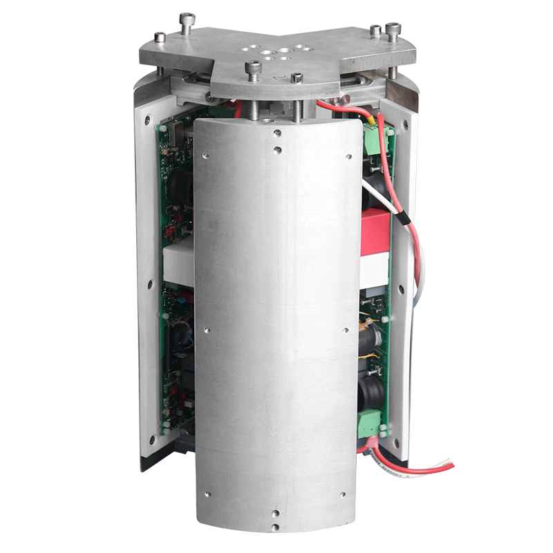
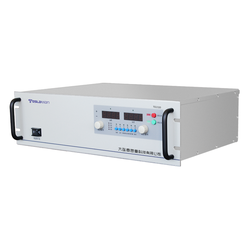
In the realm of physical vapor deposition (PVD), sputtering, and plasma-enhanced chemical vapor deposition (PECVD), the high-voltage power supply is the engine that drives the plasma generation and ion acceleration processes. The move towards more sophisticated thin-film structures with precise stoichiometric, morphological, and interfacial properties has necessitated a shift from continuous DC or simple pulsed-DC regimes to advanced pulsed power technologies with精密调制 (precision-modulated) pulse periods. This article examines the application-driven rationale and technical implementation of such modulation for coating processes. The pulse period, defined as the sum of the pulse-on time (ton) and pulse-off time (toff), is a fundamental parameter in pulsed DC or bipolar pulsed sputtering. Its precise control directly influences plasma characteristics, ion energy distribution functions (IEDF), and the resulting film properties. In reactive sputtering of insulating materials like aluminum oxide or silicon nitride, precise period modulation is critical for managing the target poisoning effect. By carefully tailoring the ton/toff ratio and the overall frequency, the power supply can allow time for the discharge of accumulated charge on the target surface during the off period, preventing arcs and maintaining a stable process. This modulation requires power supplies capable of extremely fast voltage transitions and precise timing control, often in the microsecond to nanosecond range. For plasma-enhanced processes, the pulse period modulation serves as a knob to control ion bombardment energy independently of the plasma density. During the on-time, a high negative voltage attracts ions to the substrate, influencing film density and stress. The off-time allows for plasma relaxation and neutral species diffusion. By modulating these periods, one can engineer films with low stress, high density, or graded interfaces. For example, a longer off-time at the initial stage of deposition can promote adhesion layer formation, while a subsequent shift to a different period can optimize bulk film growth. Advanced modulation schemes involve non-symmetrical bipolar pulses or medium-frequency AC cycles with deliberate period variations. These can be used to clean substrates, enhance target utilization, or deposit multilayer nanostructures in a single pump-down cycle. The power supply must provide not only the high voltage (ranging from hundreds to several thousand volts) but also deliver highly stable and repeatable pulse shapes with minimal jitter. The synchronization of this modulation with other process parameters, such as gas flow or substrate bias, is achieved through digital communication interfaces (e.g., Ethernet-based protocols), allowing for the creation of complex, recipe-driven deposition profiles. This level of control enables the deposition of films with tailored optical, electrical, and mechanical properties—such as transparent conductive oxides, hard coatings, and diffusion barriers—that meet stringent industrial specifications. The technical challenges include managing electromagnetic interference (EMI) from rapid switching, ensuring thermal stability of the power components, and developing robust algorithms for arc handling and recovery seamlessly integrated within the modulated pulse pattern. Ultimately, the precision modulation of the high-voltage pulse period transcends simple power delivery; it becomes a direct tool for plasma chemistry and physics manipulation, enabling breakthroughs in coating performance and process reproducibility for cutting-edge applications in optics, semiconductors, and functional surfaces.