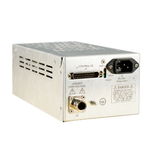
High-Voltage Power Supply for Ion Implantation Wafer Thermal Budget Control
Ion implantation is a fundamental doping process in semiconductor manufacturing. As device geometries shrink to the nanoscale, the thermal budget—the cumulative thermal exposure a wafer undergoes during processing—becomes a critical constraint. Excessive thermal exposure can cause undesirable dopant diffusion, degrading junction abruptness and device performance. This article examines the pivotal role of high-voltage power supplies in managing the wafer's thermal load during the implantation process itself, a factor often overshadowed by post-implant anneal considerations. The thermal input during ion implantation originates primarily from the kinetic energy of the incident ion beam. While this is inherent to the process, the electrical power delivered to the wafer substrate via the beam and the substrate biasing system constitutes a significant and often controllable source of localized heating. An advanced high-voltage power supply for the wafer platen (substrate holder) is engineered not just to provide a suppression or extraction bias, but to actively participate in thermal management. The traditional role of the platen power supply is to establish a potential to either repel secondary electrons (suppression) or to influence the implanted ion energy. However, the electrical current flowing to the wafer—comprising the ion beam current itself, secondary electron currents, and currents from plasma flood systems for charge neutralization—interacts with this bias voltage, depositing Ohmic (I²R) heating power directly into the wafer. A sophisticated power supply operates in a constant-voltage mode with a highly responsive current monitoring and management system. By precisely regulating the voltage in the face of fluctuating beam currents, it minimizes unnecessary power dissipation. More importantly, for thermal budget control, some systems employ dynamic bias modulation. During the implant of a die or a wafer sector, the power supply can rapidly adjust the bias voltage in a pre-programmed manner. For instance, a slightly modified bias can alter the trajectory of low-energy secondary electrons, redirecting their energy deposition away from sensitive device structures. Furthermore, the power supply's architecture can be designed for efficiency. Switching topology supplies with high efficiency (>90%) generate less waste heat within the implanter's electronics, indirectly reducing the thermal load on the tool's cooling systems, which ultimately stabilize wafer temperature. The most direct thermal interaction is through the management of the beam incident power. While the acceleration high-voltage supply (the terminal supply for medium-current implanters or the RF power for high-energy systems) sets the ion energy, its stability is again crucial. Energy fluctuations cause varying energy deposition depths and rates, leading to non-uniform thermal profiles. A stable acceleration supply ensures a consistent, predictable heating source. In cluster implant processes or when using high-current beams for source-drain extensions, wafer cooling systems (often cryogenic or backside gas-cooled chucks) work in concert with the bias supply. The power supply's controller can communicate with the thermal chuck controller. If sensors indicate a localized temperature rise at the wafer's edge (a common hotspot), the bias supply could momentarily adjust parameters for that region (in a multi-zone platen system) to redistribute electrical power dissipation, aiding the cooling system. This closed-loop thermal management, with the high-voltage supply as an active actuator, allows for tighter control of the wafer temperature throughout the implant cycle. By minimizing peak temperatures and spatial gradients, it reduces the transient thermal diffusion that occurs during the implant itself. This is particularly vital for advanced materials like strained silicon or finFET structures, which are highly sensitive to thermal stress. Therefore, a thermal-budget-aware high-voltage power supply for ion implantation is characterized by ultra-stable output to prevent variable heating, efficient power conversion to minimize system heat, and the capability for dynamic, sensor-informed modulation of its output parameters. This integrated approach helps preserve sharp doping profiles, maintains material integrity, and contributes directly to the yield and performance of leading-edge semiconductor devices.