High-Voltage Modulation for Superlattice Coating via Magnetron Sputtering
The deposition of superlattice coatings, characterized by alternating nanoscale layers of different materials, demands exceptional control over the growth process to achieve the desired periodic structure and interfacial sharpness. In magnetron sputtering systems, which are widely employed for this purpose, the introduction of high-voltage modulation techniques has revolutionized the ability to tailor film properties at the atomic level. This approach involves the application of precisely timed, variable high-voltage signals to the sputtering target or the substrate, moving beyond the traditional continuous DC or mid-frequency AC power delivery. The core objective is to exert active control over the energy and flux of ions arriving at the growing film surface, parameters that fundamentally govern nucleation, adatom mobility, and layer-by-layer growth.
One primary application is pulsed DC magnetron sputtering, where a negative high-voltage pulse train is applied to the target. By modulating the pulse frequency, width, and amplitude, it is possible to manage charge accumulation on insulating targets and also influence the plasma discharge characteristics. For reactive sputtering of compound superlattices (e.g., nitrides, oxides), this modulation helps prevent arcing and target poisoning, leading to more stable processes and stoichiometrically accurate alternating layers. More advanced techniques involve superimposing a high-voltage bias directly onto the substrate in a synchronized or asynchronous manner relative to the target pulses. This independent substrate bias modulation allows for periodic bombardment of the depositing film with ions of controlled energy. During the deposition of one layer, a specific bias condition can be applied to promote dense, crystalline growth, while during the deposition of the next material, the bias can be altered or turned off to minimize intermixing or to preserve a specific metastable phase.
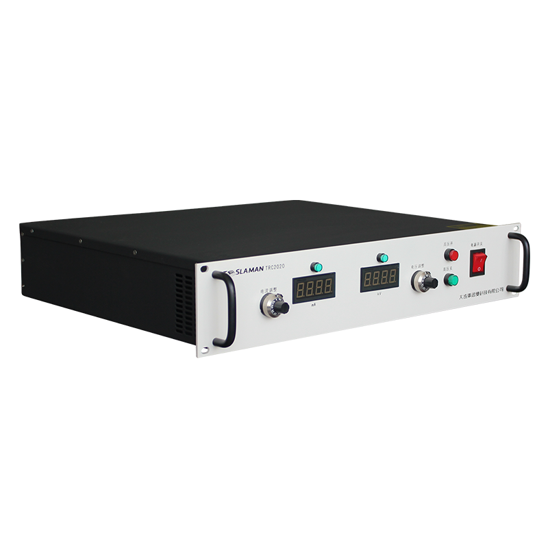
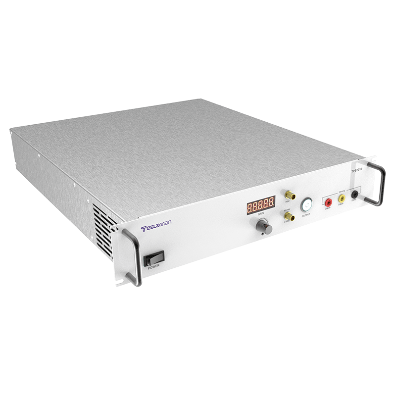
The design of the high-voltage modulation power supply is critical. It must deliver fast-rising and falling voltage pulses with minimal overshoot and ringing to ensure clean temporal separation of deposition and bombardment phases. The switching frequencies can range from tens of kilohertz to several hundred kilohertz, requiring robust solid-state switching architectures using MOSFET or IGBT stacks. Voltage amplitudes for target pulsing can reach -1 to -2 kV, while substrate bias modulation may range from a few tens to hundreds of volts, either DC or pulsed. The synchronization between multiple modulated power supplies—one for the target and one or more for the substrate—is managed by a master controller that follows a pre-programmed deposition recipe. This precise orchestration enables the engineering of interfaces with minimized defects, controlled residual stress, and optimized functional properties such as hardness, thermal stability, and electronic behavior in the final superlattice coating. Thus, high-voltage modulation transforms the magnetron sputtering process from a passive deposition tool into an active synthesis platform for advanced nanomaterials.