High-Voltage Design for Multilayer Ceramic Electrodes in Electrostatic Chucks
Electrostatic chucks (ESCs) are the principal wafer-clamping technology in modern semiconductor fabrication equipment, providing secure, particulate-free holding during processes like plasma etching, chemical vapor deposition, and ion implantation. The evolution towards multilayer ceramic electrode structures within the chuck body represents a significant advancement, demanding a correspondingly sophisticated high-voltage power supply design to unlock their full potential in thermal management, process uniformity, and reliability.
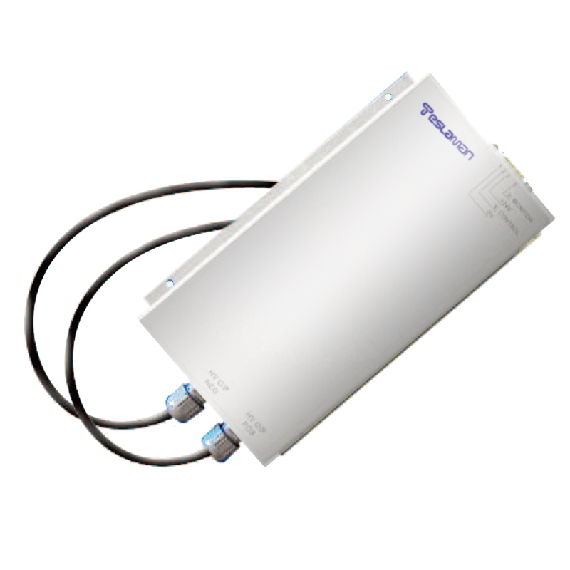
The core of a multilayer ceramic ESC is a complex laminate of alternating conductive electrode layers and insulating ceramic layers, typically aluminum nitride (AlN) or alumina. This buried electrode architecture allows for the creation of complex electrostatic field patterns, such as bipolar (Johnsen-Rahbek or Coulombic) or multipolar arrangements, from a monolithic chuck body. The high-voltage supply must not only provide the clamping potential, typically ranging from 500V to 3kV for bipolar designs, but it must do so with precise control over multiple independent output channels. Each channel corresponds to a distinct electrode zone within the chuck, enabling advanced features like zoned clamping force control or active thermal regulation through the electrostatically modulated thermal boundary resistance.
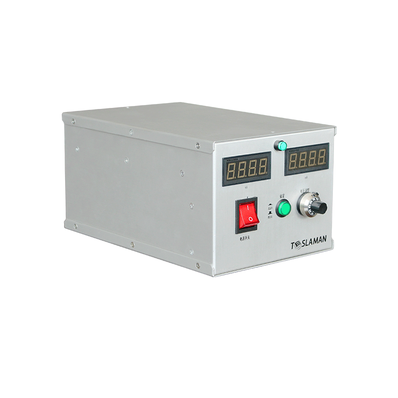
A critical requirement is the rapid and stable application and removal of the clamping voltage. During wafer transfer, the voltage must be ramped down to zero quickly and reliably to release the wafer, but any residual charge can cause wafer sticking or misalignment. The power supply must incorporate active discharge circuits that can sink current from the highly capacitive electrode layers, ensuring the chuck potential reaches a true zero within a specified time, often less than 100 milliseconds. Conversely, when clamping, the voltage must ramp up in a controlled manner to prevent arcing or excessive initial force that could damage backside films on the wafer. This necessitates programmable slew rate control within the supply itself.
The interaction with plasma in etch and deposition tools adds immense complexity. The chuck, and by extension its power supply, becomes part of the RF return path for the plasma excitation circuit. The high-voltage DC clamping supply must be effectively isolated from the MHz or kHz RF potentials present on the chuck surface. This is achieved through sophisticated filtering networks—combinations of inductors, capacitors, and ferrite beads—integrated at the output of each high-voltage channel. These filters must present a high impedance at the RF frequency to block RF from entering and damaging the DC supply, while offering a low-impedance path for the DC clamping voltage. Any imperfection in this filtering can lead to modulation of the clamping force at the RF frequency, causing wafer vibration, or can allow RF rectification that creates unwanted DC offsets, compromising process repeatability.
Thermal management is intrinsically linked to the high-voltage design. In monopolar or bipolar Johnsen-Rahbek chucks, the clamping mechanism relies on a minute current flow through the slightly conductive ceramic. The power supply must regulate this current with high precision, as it directly influences both the clamping force and the heat generated at the wafer-chuck interface. For temperature-controlled chucks, a separate heater electrode layer is often powered by a different high-current, lower-voltage supply, but the clamping and heating circuits must be co-designed to prevent capacitive or inductive coupling that could cause instability. In advanced systems, the clamping voltage on specific zones can be dynamically adjusted in a closed loop with temperature sensors to correct for process-induced thermal non-uniformities across the wafer.
Reliability under continuous operation in a harsh environment is non-negotiable. The power supply must be designed to withstand occasional arcs from plasma instability or wafer backside defects. This requires fast-responding arc detection circuitry that can momentarily disable the output within microseconds and implement a pre-programmed recovery sequence. Furthermore, the ceramic electrode structure itself has a finite dielectric strength and leakage characteristics that change with temperature and exposure to process chemistries. The power supply should include continuous monitoring of leakage current to ground for each electrode zone, providing an early diagnostic for ceramic degradation, contamination buildup, or coolant leaks before catastrophic failure occurs. This data is logged for predictive maintenance, aligning the high-voltage system's health with overall tool uptime and wafer yield.