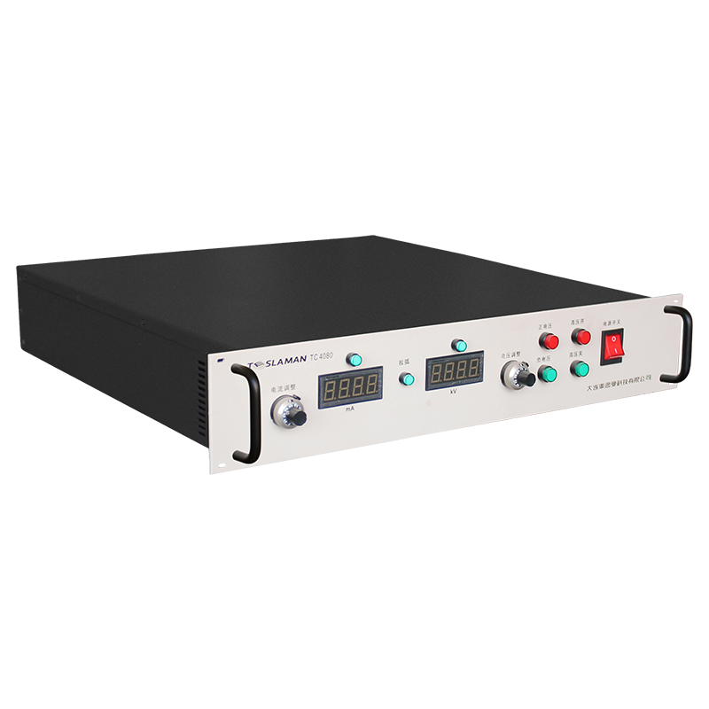
High-Voltage Precision Control for Focused Ion Beam Circuit Repair
Focused Ion Beam (FIB) systems have become indispensable tools for the failure analysis, prototyping, and repair of integrated circuits. The process involves using a finely focused beam of gallium ions to precisely mill away material or to induce localized deposition of conductive or insulating layers. The quality and precision of these operations, especially when working on modern nanoscale circuitry, are profoundly dependent on the high-voltage power supplies that control the ion beam. These are not simple power sources; they are ultra-stable, low-noise precision instruments responsible for beam acceleration, shaping, and deflection.
The primary high-voltage supply accelerates ions from the source to energies typically ranging from 1 keV to 30 keV. The stability of this acceleration voltage is paramount. Any drift or noise directly translates into a change in the ion landing energy, which affects the sputtering yield—the volume of material removed per incident ion. A fluctuation of even 0.1% can lead to visible non-uniformities during cross-section milling or cause over-milling when attempting to cut through a specific layer. Therefore, the acceleration power supply must exhibit long-term drift measured in parts per million per hour and output ripple in the millivolt range. This requires the use of ultra-stable voltage references, low-temperature-coefficient precision resistors in feedback networks, and advanced regulation topologies that actively cancel residual AC components.
Beyond the main acceleration voltage, a suite of other high-voltage supplies controls the electrostatic lenses and the deflection system. The electrostatic lenses, which focus the beam down to a spot size often smaller than 10 nanometers, require supplies with similar stability specifications. A change in a lens voltage alters the focal length, defocusing the beam and drastically reducing spatial resolution. This is particularly critical during Gas Injection System (GIS) assisted deposition, where a defocused beam can create a broad, poorly defined conductive line instead of a sharp via fill. The deflection plates, which raster the beam across the sample, are driven by high-voltage amplifiers. The precision here relates to linearity and bandwidth. Non-linearity in the amplifier output causes geometric distortion in the milled pattern—a square shape might become barrel-shaped. Limited bandwidth results in slow settling times at the edges of a raster, causing rounded corners or smearing. For circuit edit operations that involve cutting or depositing lines with sub-micron alignment to existing features, these imperfections are unacceptable.
A critical, often overlooked, aspect is the interaction between these supplies. Ground loops, crosstalk, and load transients from one supply can inject noise into another. For example, a rapid voltage swing on a deflection plate can momentarily perturb the acceleration voltage through capacitive coupling or through a shared ground impedance. Sophisticated FIB power supply systems employ fully isolated, digitally controlled modules with local regulation and optical or isolated digital communication links to the main controller. This star-point grounding and isolation strategy minimizes interactive noise.
Furthermore, the control software integrates these supplies into a coordinated system. For a trench milling operation, the software may dynamically adjust lens voltages (dynamic focus) as the beam is deflected to the edge of the field to compensate for field curvature. It may also synchronize the beam blanking voltage with stage movements or gas injector pulses. The calibration of these supplies against internal or external standards is a routine but vital maintenance task, ensuring that the commanded voltage corresponds accurately to the actual field applied to the beam. In essence, the high-voltage precision control system in a FIB workstation is the foundation of its nanoscale machining capability. It translates digital design data into physical actions on the circuit with atomic-level precision, enabling the repair of million-dollar semiconductor masks, the creation of prototypes for new chip designs, and the diagnostic cross-sectioning that reveals the root cause of elusive circuit failures.