Closed-Loop High-Voltage Control for Ion Implantation Dose Uniformity
Ion implantation is a critical doping process in semiconductor manufacturing, where achieving a uniform dopant concentration across the entire wafer surface is paramount for device performance and yield. Traditional systems rely on open-loop control of beam scanning and wafer mechanical movement, assuming a stable, uniform beam current density. However, beam fluctuations, space charge effects, and chamber pressure variations can introduce dose non-uniformities exceeding 1%, which is unacceptable for advanced nodes. Closed-loop high-voltage control addresses this by using real-time, in-situ sensors to measure the actual dose being delivered and dynamically adjusting the beam acceleration or scanning parameters to correct deviations.
The core of this system is the integration of non-invasive, high-speed dose sensors. Faraday cups are traditionally used for beam current measurement, but they are typically placed at the wafer edge and only provide a periodic sample. For true closed-loop control, an array of miniature Faraday cups or specialized non-intercepting sensors, such as capacitive beam position monitors or electron flood gun charge neutralization monitors, are embedded in the wafer platen itself. These sensors provide a spatially resolved map of the ion flux incident on the wafer in real-time. As the wafer scans through the beam, the sensor array generates a high-resolution dose map.
The control algorithm compares this real-time map to the target dose profile. Any discrepancy, such as a region receiving a higher-than-average flux, generates an error signal. This error signal is then fed back to adjust the high-voltage subsystems that govern the beam. There are two primary actuation points. The first is the beam scanning system. The high-voltage amplifiers that drive the electrostatic or magnetic beam deflection plates can be commanded to slightly modulate the scanning speed. If a sensor indicates a local overdose, the algorithm can instruct the scanner to increase the beam velocity over that corresponding region on the next scan pass, effectively reducing the dwell time and integrated dose.
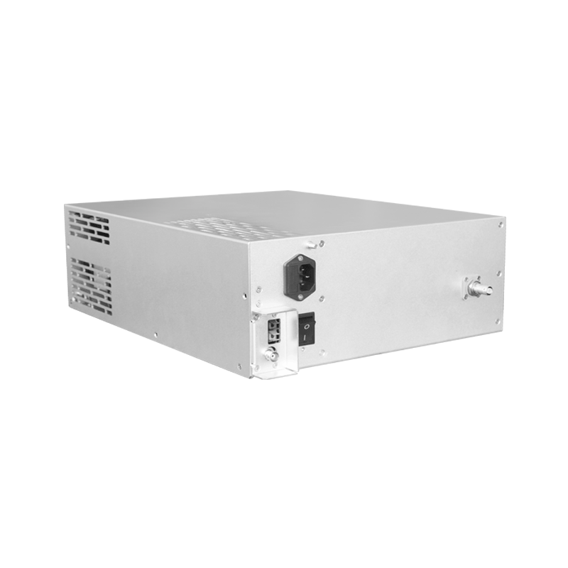
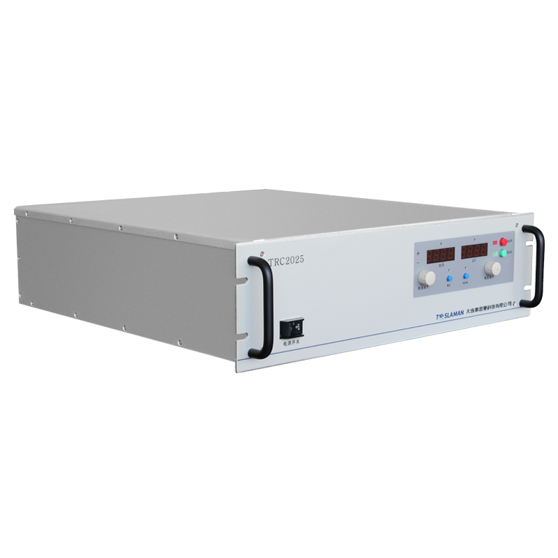
The second, more direct actuation point is the beam energy itself. The final acceleration voltage, supplied by the high-voltage deck, directly influences the beam's trajectory through the mass analyzing magnet and its subsequent focus. By making minute, rapid adjustments to this acceleration voltage (on the order of tens of volts within a tens of kilovolt baseline), the beam's position or shape at the wafer plane can be subtly steered or defocused to smear out non-uniformities. This requires a high-voltage supply with exceptionally fast regulation and low noise, as the corrections must be applied within the timeframe of a single scan line to be effective.
Implementing this closed-loop system presents substantial engineering challenges. The sensors must survive in the harsh environment of the implant chamber, withstanding ion bombardment and maintaining calibration. The data acquisition system must have sufficient bandwidth to process signals from multiple sensors at the scanning frequency, which can be in the kilohertz range. The control loop's latency—from sensor measurement to high-voltage adjustment—must be minimized and deterministic. Any delay introduces a spatial lag between the detected error and the applied correction, potentially making the non-uniformity worse if not properly compensated.
Furthermore, the system must be intelligent enough to distinguish between true dose errors and transient signals from, for example, a passing ionized gas molecule or a secondary electron emission event. This involves signal processing with filtering and validation algorithms. The closed-loop controller also needs to be adaptive, as the relationship between a change in acceleration voltage and the resulting change in beam profile is not linear and can vary with beam species, total beam current, and vacuum conditions. Advanced systems employ a model-predictive control approach, using a physics-based model of the beamline to predict the outcome of a control action before applying it.
The ultimate benefit is a dramatic reduction in within-wafer and wafer-to-wafer dose variation, pushing uniformity well below 0.5%. This directly improves transistor threshold voltage matching, reduces parametric yield loss, and enables tighter design rules. The high-voltage power supply, in this context, evolves from a static energy source into the key actuator in a high-speed, precision feedback loop, where its stability and dynamic response become the limiting factors for achieving atomic-level doping accuracy across 300mm silicon wafers.