Multi-Phase High-Voltage Drive Strategy for Zoned Electrostatic Chucks
Electrostatic chucks (ESCs) are essential for wafer clamping in plasma processes. As wafer sizes increase and process demands for thermal uniformity become more stringent, the traditional approach of using a single, uniform electrode or a simple bipolar design reaches its limits. A multi-phase high-voltage drive strategy, where the chuck electrode is divided into multiple independent zones powered by phase-shifted or independently programmed AC or pulsed DC waveforms, offers a revolutionary method for controlling clamping force distribution, managing wafer temperature, and suppressing process-induced non-uniformities.
In this architecture, the chuck contains several electrode sectors, often arranged concentrically or in a hexagonal grid. Each sector is connected to its own high-voltage output channel from a multi-channel power supply. Unlike DC clamping, where a static field is applied, the multi-phase strategy applies time-varying potentials. One common implementation uses three-phase AC voltages. Each electrode zone is driven by a sinusoidal high-voltage waveform (e.g., at a frequency of 0.1 to 10 kHz), with a 120-degree phase shift between adjacent zones. This creates a rotating electric field at the wafer interface. The primary advantage is the elimination of static charge buildup that can occur with DC on insulating films, which can lead to unpredictable sticking or particle contamination during wafer release.
Beyond solving de-chucking issues, the independent control of each zone's voltage waveform provides powerful levers for process control. During a plasma etch step, the plasma sheath potential and ion flux are not perfectly uniform across the wafer, often leading to an center-to-edge etch rate profile. By independently adjusting the amplitude or phase of the voltage on edge zones versus center zones, the electrical boundary condition presented by the chuck can be altered. This, in turn, influences the local plasma sheath thickness and ion energy, providing a knob to actively correct etch rate non-uniformity. This is a form of active edge compensation that is far more responsive than passive hardware modifications.
Thermal management is another key application. In a multi-zone chuck with independent DC or low-frequency AC control, the clamping force—and consequently the thermal contact resistance—can be varied from zone to zone. By slightly increasing the clamping force in a region that is running cooler than desired (as measured by embedded temperature sensors), the thermal conductance to the cooled chuck base is improved, raising that zone's temperature. Conversely, reducing the force in a hot spot increases thermal resistance, allowing it to cool. This dynamic thermal zoning requires a high-voltage supply capable of modulating each channel's output with fine resolution in response to a real-time thermal map.
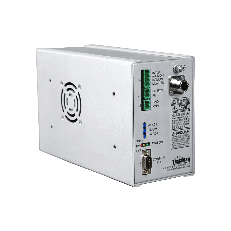
The design of the multi-phase high-voltage supply is highly complex. Each channel must provide kilovolt-level outputs with precise control over amplitude, frequency, and phase relative to a master clock. The channels must be perfectly isolated from each other to prevent any cross-coupling that would destroy the intended phase relationships. This isolation extends to both power and control, necessitating isolated gate drivers and communication via fiber optics or isolated digital links. The output stages must handle the capacitive load of the chuck electrodes, which can be significant, without introducing distortion or phase lag in the waveforms.
Reliability and fault tolerance are critical. The system must be designed such that the failure of a single drive channel does not cause a total chuck failure or create a dangerous asymmetry. Redundant components and the ability to gracefully degrade performance (e.g., by switching a faulty zone to a backup channel or a safe default voltage) are essential. Furthermore, the interaction between these time-varying chuck potentials and the MHz or kHz RF bias applied to the wafer for plasma generation must be carefully managed through filtering and shielding to prevent intermodulation products that could disrupt the plasma or damage the power supplies.
This multi-phase, multi-zone drive strategy transforms the electrostatic chuck from a simple clamping device into an active, programmable surface that interacts intelligently with both the wafer and the plasma. It provides process engineers with a set of electrical actuators to combat inherent non-uniformities, pushing the limits of uniformity for critical dimensions, film thickness, and material properties across the wafer, which is fundamental for the yield of leading-edge semiconductor devices.