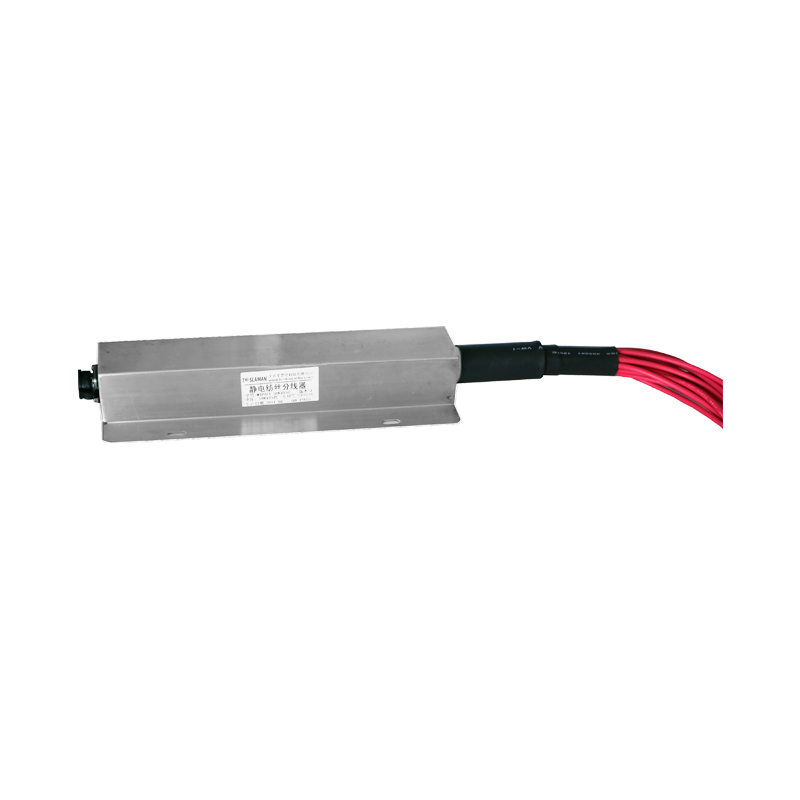
High-Voltage Precursor Control for Focused Ion Beam Induced Deposition
Focused Ion Beam (FIB) Induced Deposition is a nanoscale additive manufacturing technique used for circuit edit, mask repair, and prototyping of micro-devices. A precursor gas, such as a metal-organic compound or tungsten carbonyl, is introduced via a micro-capillary near the sample surface. A finely focused beam of gallium ions then scans the area, dissociating the adsorbed precursor molecules and depositing a solid material (metal or insulator) while volatilizing the organic ligands. The deposition rate, purity, and resistivity of the resulting deposit are highly sensitive to the local gas flux and the ion beam parameters. Precise control of the gas delivery system, which often involves electrostatic manipulation of the gas molecules themselves, is therefore critical, and this is where specialized high-voltage control plays a subtle yet vital role.
The precursor gas molecules are typically polar or can be polarized. As they emanate from the nozzle, they form a cloud or flux directed towards the substrate. Uncontrolled, this cloud is diffuse, leading to poor deposition efficiency and significant parasitic deposition on surrounding areas. To enhance localization and efficiency, an electrostatic field can be applied between the gas injector nozzle and the substrate. By biasing the nozzle with a moderate high voltage (typically a few hundred volts to a few kilovolts, either DC or pulsed), the polar gas molecules experience a force, directing them more strongly towards the focused ion beam impact point. This effectively increases the local precursor concentration exactly where it is needed, improving the deposition rate and reducing the required ion dose, which minimizes Ga+ implantation and damage to the underlying substrate.
This high-voltage control must be exquisitely synchronized with the ion beam scanning and the gas valve pulse. The gas delivery is often pulsed to conserve precursor and minimize chamber contamination. The high voltage on the nozzle is therefore also pulsed, being applied only during the brief window when the gas pulse arrives and the ion beam is dwelling on the deposition pixel. The rise and fall time of this voltage pulse must be fast to match the gas pulse envelope. Any lag can result in gas being directed to the wrong location or being inefficiently used.
Furthermore, the voltage polarity and magnitude are process-dependent. For depositing insulating materials like silicon dioxide from a TEOS precursor, a different field configuration might be optimal compared to depositing platinum from a (CH3)3Pt(CpCH3) precursor. The field strength influences not just the trajectory but also the kinetic energy with which molecules adsorb on the surface, which can affect the initial sticking coefficient and the subsequent surface diffusion before dissociation. In some advanced systems, separate electrodes near the sample stage, biased with independent voltages, are used to shape the electrostatic field, creating a more focused gas flux pattern.
The high-voltage controller for this application is a low-current, precision instrument. It must be immune to the noisy environment of the FIB chamber, where secondary electron detectors and stage motors create electrical interference. Its output must be stable and ripple-free, as fluctuations would cause jitter in the gas flux, leading to non-uniform deposition thickness. Integration with the FIB's main control software is seamless, allowing the gas field voltage to be defined as a parameter within the deposition recipe, alongside beam current, dwell time, and pattern geometry.
This electrostatic enhancement of precursor delivery directly enables higher-quality FIB deposits. It results in lower resistivity metallic lines, more stoichiometric insulating layers, and sharper feature definition. It expands the process window, allowing for successful deposition on non-planar or complex topography. By leveraging high-voltage control over a seemingly mundane gas delivery step, the technique of Ion Beam Induced Deposition gains a critical dimension of control, pushing its capabilities further into the realm of reliable, high-fidelity nanofabrication for the most demanding applications in semiconductor failure analysis and microsystem development.