High-Voltage Sequencing for Rapid Pick-and-Place in Electrostatic Chucks
The handling of thin, fragile substrates such as silicon wafers or glass panels in vacuum environments presents a unique set of mechanical and electrical challenges. For the past five decades, I have observed the gradual but definitive shift from purely mechanical clamping methods to the widespread adoption of electrostatic chucks. These devices, which use the force of an electrostatic field to hold a substrate firmly in place, have become indispensable in processes like etching, deposition, and lithography. However, the operational cycle of an electrostatic chuck is not as simple as applying a voltage and walking away. It demands a carefully orchestrated high-voltage sequence to enable rapid, damage-free pick-and-place operations, a requirement that has pushed the boundaries of high-voltage power supply design.
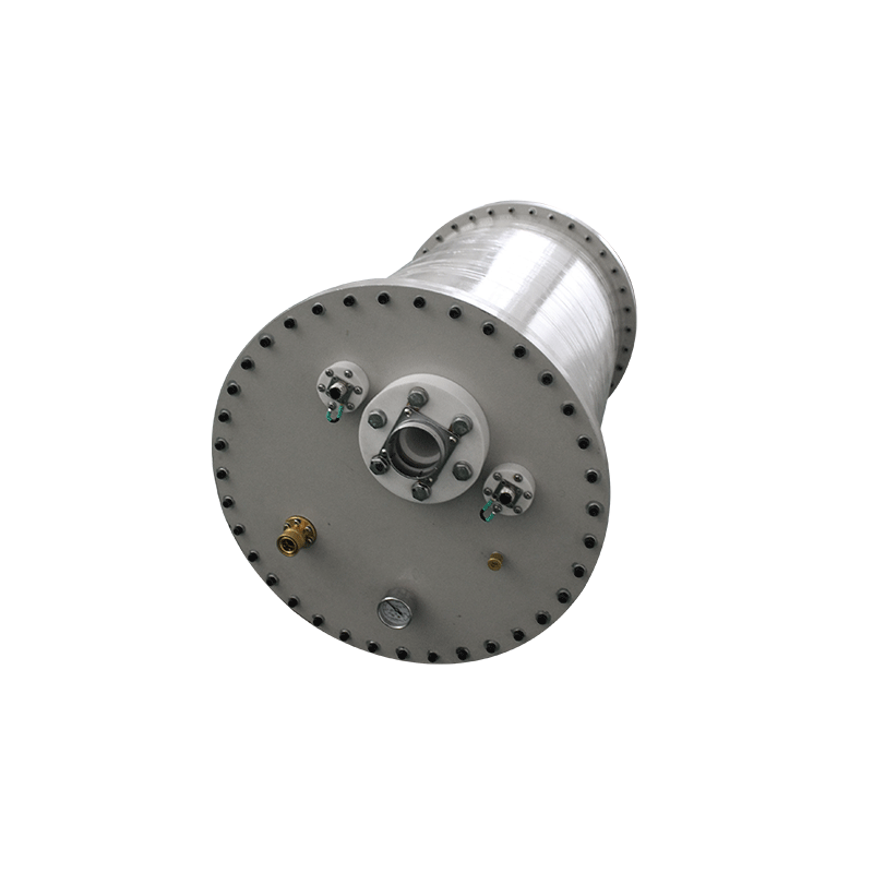
The underlying principle of an electrostatic chuck is the generation of an attractive force between the chuck body and the substrate. This is achieved by embedding one or more electrodes within a dielectric material and applying a high voltage, typically in the range of several hundred to several thousand volts, between these electrodes. The electric field polarizes the material of the substrate and the dielectric, inducing bound charges that result in a strong clamping force. The magnitude of this force is proportional to the square of the applied voltage. For rapid processing, such as in a cluster tool where wafers are moved from one chamber to another every few seconds, the chuck must be able to clamp and declamp the wafer with precision and speed.
The challenge lies primarily in the declamping phase. When a high voltage is applied, the electric field not only creates the clamping force but also causes charge to accumulate in the dielectric material and on the substrate surface. When the power supply is simply turned off, this trapped charge does not instantly disappear. It remains, holding the wafer in place with a residual force known as electrostatic residual attraction or stiction. In a high-throughput manufacturing environment, waiting for this charge to decay naturally, which could take many seconds or even minutes, is unacceptable. Therefore, the high-voltage supply must be capable of executing a specific sequence designed to actively and rapidly neutralize this trapped charge.
The classic solution, and one I have refined in my own work, is the use of a bipolar clamping and declamping sequence. The chuck electrodes are often arranged in an interdigitated pattern or as a pair of separate electrodes. During the clamping phase, a positive high voltage is applied to one set of electrodes and a negative high voltage to the other. This creates a strong, uniform clamping field. To declamp, the power supply does not simply switch off. Instead, it executes a rapid reversal of the applied voltages, momentarily applying a negative voltage to the electrodes that were positive and a positive voltage to those that were negative. This reversal creates a field opposite to the original polarizing field, actively sweeping the trapped charge out of the dielectric and neutralizing the residual attraction. The speed and shape of this voltage reversal are critical. It must be fast enough to be effective before any thermal or mechanical relaxation can occur, but it must be carefully controlled to prevent dielectric breakdown or arcing within the chuck structure.
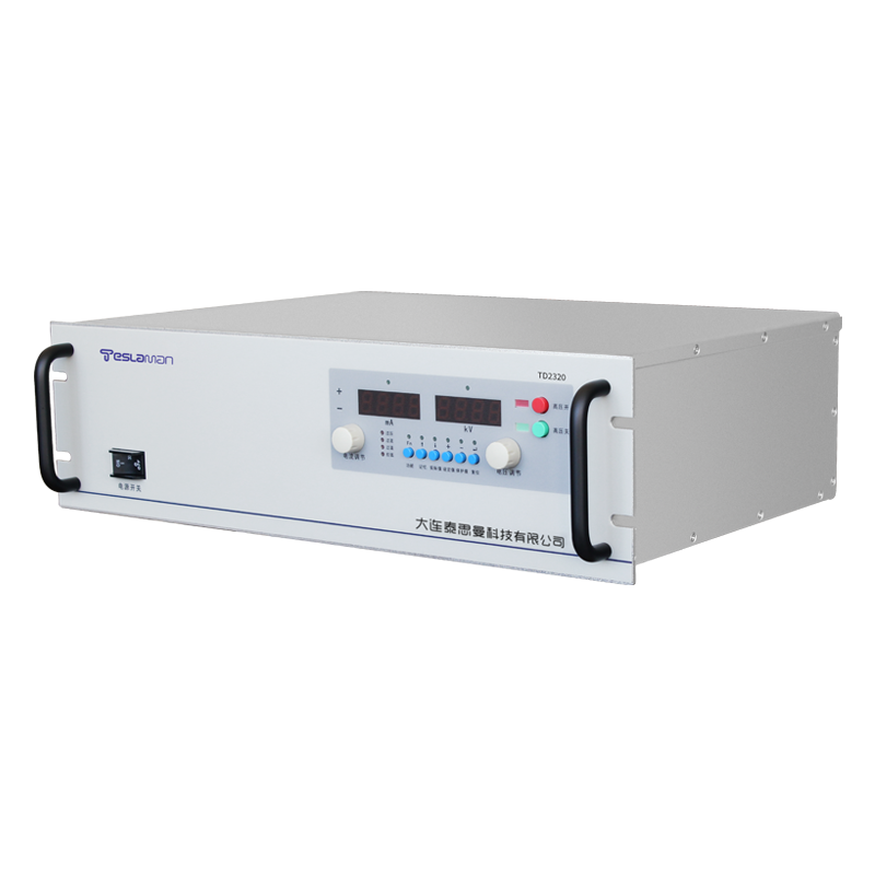
The power supply responsible for this sequence must therefore be a highly agile, bipolar high-voltage amplifier. It must be capable of switching from a positive high voltage to a negative high voltage, often with a brief zero-voltage pause in between, within milliseconds. The current delivery capability during this transition is also important. As the voltage swings, it must charge and discharge the capacitance of the chuck and the wafer, which can be substantial. This requires a power supply with a robust output stage capable of sourcing and sinking significant peak currents. The design of the output switches, typically a bridge configuration of IGBTs or MOSFETs, must be optimized for this bidirectional power flow.
Beyond the simple bipolar reversal, more sophisticated sequences have been developed to address the specific characteristics of different dielectric materials and substrate types. For chucks using materials with high volume resistivity, such as alumina or certain polymers, the charge trapping can be particularly persistent. In these cases, a multi-pulse sequence can be employed. This might involve applying a series of alternating polarity voltage pulses of decreasing amplitude, effectively shaking the charge loose from deep trap states. Alternatively, a slow, ramped AC voltage can be applied to the chuck after the main clamping voltage is removed, gently agitating the trapped charge until it recombines or is conducted away.
The timing of this high-voltage sequence must be synchronized with the mechanical motion of the robot handling the wafer. The declamping sequence must be initiated just before the robot lifts the wafer. The supply must provide a feedback signal, perhaps a measurement of the current flowing during the declamping phase, to confirm that the charge has been sufficiently neutralized. A sudden lack of current might indicate that the wafer has already lifted off or that there is a contact issue. This feedback is integrated into the tool's safety interlock system to prevent the robot from attempting to lift a still-clamped wafer, which could shatter the substrate or damage the robot.
In my consultations with equipment manufacturers, I have also seen the evolution towards chucks with multiple, individually addressable zones. This allows for differential clamping force across the wafer, which can be used to compensate for wafer warpage or to improve thermal contact with the chuck in specific areas. The power supply for such a chuck is essentially a multi-channel high-voltage system, with each channel capable of executing its own independent clamping and declamping sequence. The coordination of these sequences becomes a complex control problem, ensuring that the net force on the wafer is always balanced to prevent bowing or fracture. The high-voltage sequencing, therefore, moves from a simple on-off or bipolar reversal to a carefully choreographed dance of voltages across multiple electrodes, all within the span of a few seconds, a testament to the sophistication that modern power electronics brings to seemingly simple mechanical handling tasks.