Precise Control Research for Voltage Ramp Rate in Electrostatic Chuck High Voltage Power Supply
Electrostatic chucks have become essential tools in semiconductor manufacturing for holding wafers during various processing steps. The electrostatic chuck uses high voltage to create an electrostatic force that holds the wafer securely. The voltage ramp rate, or how quickly the chuck voltage changes, is a critical parameter that affects both process results and wafer safety. Too rapid voltage changes can cause excessive electrostatic forces that may damage the wafer or chuck. Too slow voltage changes can increase process time and reduce throughput. Precise control of the voltage ramp rate is essential for optimizing the trade-off between process speed and wafer safety.
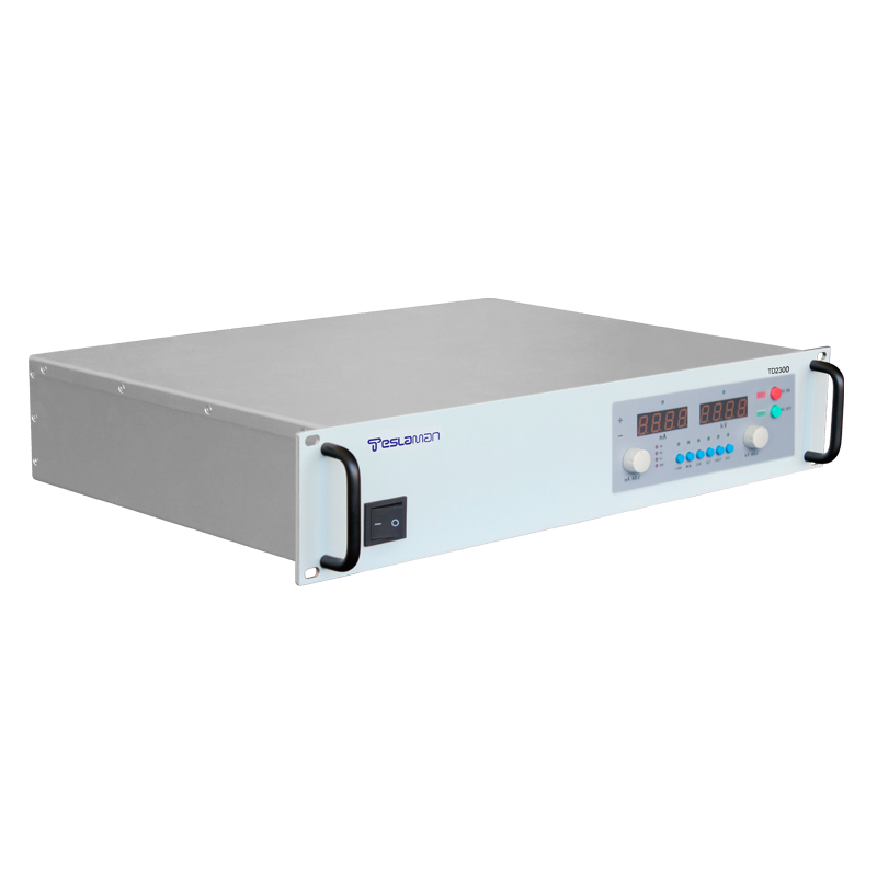
The electrical requirements for electrostatic chuck power supplies depend on the specific chuck design and process requirements. Typical operating voltages range from 500 to 3000 volts, with currents from microamperes to milliamps depending on chuck size and wafer characteristics. The power supply must provide stable output across these operating ranges while accommodating the varying load presented by the chuck. The load varies with wafer presence, chuck temperature, and surface conditions, requiring the power supply to adapt to these variations while maintaining precise control of voltage ramp rate.
Voltage ramp rate affects multiple aspects of chuck operation. During chucking, the voltage must ramp from zero to the operating level to establish the electrostatic force. The ramp rate during this phase affects how quickly the wafer becomes securely held. During dechucking, the voltage must ramp down to release the wafer. The ramp rate during this phase affects how quickly the wafer can be removed. During process adjustments, the voltage may be ramped to different levels to adjust the chucking force. The ramp rate during these adjustments affects how quickly the process can adapt to changing conditions.
Wafer safety considerations place upper limits on acceptable voltage ramp rates. Excessive electrostatic forces can cause wafer damage including cracking, breakage, or generation of particles that can contaminate the wafer. The maximum safe ramp rate depends on multiple factors including wafer thickness, material properties, chuck design, and process conditions. Advanced systems may implement adaptive ramp rates that adjust based on wafer characteristics. The safety limits must be carefully characterized and enforced by the power supply control algorithms.
Chuck design affects the achievable voltage ramp rates. Different chuck designs have different capacitance characteristics and force generation mechanisms. Some chuck designs may be more tolerant of rapid voltage changes than others. The chuck mechanical design also affects how quickly forces can be applied without causing damage. The power supply control algorithms must be optimized for the specific chuck design being used. Advanced implementations may automatically adapt to different chuck types.
Process requirements influence the desired voltage ramp rates. Different processes have different requirements for chucking force establishment and adjustment. Some processes require very rapid chucking to minimize process time. Other processes may require very gradual chucking to prevent process disturbances. The power supply must support a wide range of ramp rates to accommodate different process requirements. Advanced systems may store process-specific ramp rate profiles that are automatically selected based on the process being run.
Voltage ramp rate control algorithms must balance multiple competing requirements. The algorithm must achieve the desired ramp rate while maintaining voltage stability and avoiding overshoot. The algorithm must also accommodate the varying load characteristics of the chuck during voltage ramps. The algorithm must enforce safety limits while meeting process time requirements. Advanced algorithms may implement model-based control that predicts chuck behavior and optimizes ramp profiles accordingly.
Load compensation during voltage ramps is critical for maintaining control accuracy. The chuck capacitance varies during voltage ramps due to changing electric field conditions and dielectric properties. This load variation can cause the actual voltage ramp to deviate from the commanded ramp if not compensated. Advanced control algorithms actively measure and compensate for these load variations. The compensation must be fast enough to maintain accurate ramp control across the full range of operating conditions.
Voltage overshoot prevention is particularly important during voltage ramps. Overshoot can cause excessive electrostatic forces that may damage the wafer. The control algorithm must carefully manage the transition to the target voltage to avoid overshoot. Advanced algorithms may implement specialized ramp profiles that approach the target voltage asymptotically rather than with a sharp transition. The algorithm must also respond quickly to any unexpected overshoot that may occur.
Current limiting during voltage ramps protects both the power supply and the chuck. The capacitance of the chuck can draw substantial current during voltage ramps, particularly for rapid ramps. The power supply must limit this current to prevent damage to power supply components or the chuck. The current limit must be set high enough to allow the desired ramp rate but low enough to provide protection. Advanced implementations may implement adaptive current limits that adjust based on ramp rate and operating conditions.
Monitoring and feedback enable precise ramp rate control. Monitoring of actual voltage, current, and chuck force provides feedback for control algorithms. Advanced systems may monitor wafer position or other parameters to detect potential problems. The feedback enables the control algorithm to correct for deviations from the desired ramp profile. Advanced implementations may implement predictive control that anticipates required corrections based on measured conditions.
Safety interlocks prevent hazardous voltage ramp conditions. The power supply should not execute voltage ramps if safety conditions are not met. Interlocks typically verify conditions such as proper wafer presence, chuck condition, and absence of personnel in hazardous areas. The interlock systems must be designed with fail-safe principles. The interlock logic must prevent ramp rates that exceed safe limits for the specific operating conditions.
Calibration and verification ensure that ramp rate control meets requirements. Calibration procedures involve measuring actual voltage ramps under various conditions to verify that they match commanded profiles. Verification testing confirms that safety limits are enforced and that process requirements are met. The calibration and verification processes must be documented to ensure reproducibility. Regular recalibration may be required to maintain accuracy over time.
Recent advances in ramp rate control technology have improved the precision and safety of electrostatic chuck operation. Adaptive control algorithms have enabled optimization of ramp rates for specific wafers and processes. Advanced monitoring and feedback have improved control accuracy and safety. Model-based control has enabled prediction of optimal ramp profiles. These advances have directly improved process throughput while maintaining or improving wafer safety.
Emerging semiconductor manufacturing trends continue to drive innovation in ramp rate control technology. The development of larger and thinner wafers creates new challenges for safe ramp rates. Increasingly complex processes with more rapid transitions require faster and more precise ramp control. The trend toward more automated processing creates demand for algorithms with enhanced adaptive and predictive capabilities. These evolving requirements ensure continued development of voltage ramp rate control technology specifically tailored to the unique needs of electrostatic chuck high voltage power supplies.