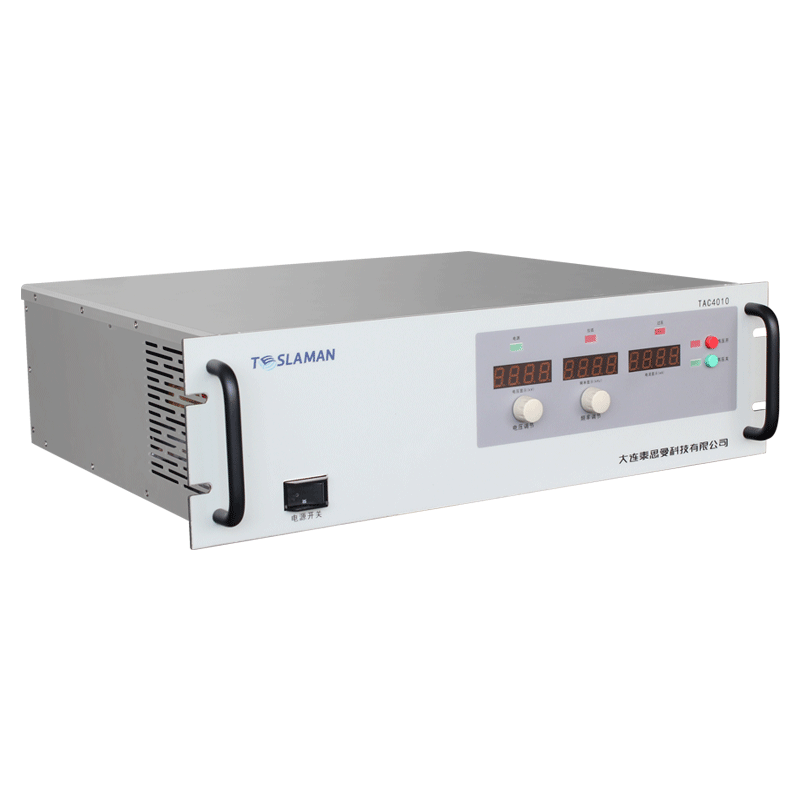
Timing of Multi-module Series High Voltage Pulse Power Supply Based on Semiconductor Switches
High voltage pulse power supplies find extensive applications in industrial, scientific, and medical fields where high-power electrical pulses are required. When the voltage requirements exceed the capability of single modules, multiple modules can be connected in series to achieve the desired output voltage. The timing coordination between these modules is critical for generating clean, well-defined pulses with the required amplitude and waveform characteristics. Semiconductor switches provide the precise control needed for timing coordination in modern pulse power systems.
The series connection of high voltage modules presents unique timing challenges. Each module contributes a portion of the total output voltage, and all modules must switch simultaneously to produce a clean pulse. Any timing mismatch between modules creates voltage imbalances and waveform distortions. In extreme cases, timing errors can cause overvoltage on some modules while others are still turning on, potentially damaging the semiconductor switches. Precise timing coordination is essential for reliable and efficient operation.
Semiconductor switches have largely replaced spark gaps and other traditional switching elements in modern pulse power supplies. Insulated gate bipolar transistors, metal-oxide-semiconductor field-effect transistors, and more recently, silicon carbide and gallium nitride devices offer advantages in controllability, repetition rate, and lifetime. These switches can be triggered with precise timing through gate drive signals, enabling the coordination required for multi-module systems.
The timing requirements for series-connected modules depend on the pulse characteristics and the application requirements. For pulses with fast rise times, the timing skew between modules must be a small fraction of the rise time to avoid waveform distortion. For applications requiring precise pulse width control, the turn-off timing must be equally well coordinated. The timing jitter, which represents the random variation in timing from pulse to pulse, must be minimized for applications requiring reproducible pulse characteristics.
Gate drive circuits translate the timing commands into the gate signals that control the semiconductor switches. The gate drive must provide sufficient gate current to charge and discharge the gate capacitance rapidly, enabling fast switching transitions. The gate drive must also provide the necessary isolation between the low-voltage control circuits and the high-voltage switch. Optical fibers or pulse transformers provide the isolation while maintaining timing precision.
Timing distribution systems deliver the trigger signals to all modules with minimal skew. The distribution can be implemented using digital communication networks, dedicated timing lines, or optical fiber links. Each approach offers different trade-offs between timing precision, cost, and complexity. The distribution system must account for propagation delays in cables and circuits, ensuring that all modules receive their trigger signals at the correct time.
Delay compensation techniques correct for inherent timing differences between modules. Each module may have slightly different response times due to component variations and circuit layout differences. Programmable delay circuits can adjust the timing of each module individually to compensate for these differences. Calibration procedures measure the timing differences and determine the appropriate compensation values. Regular recalibration maintains timing precision as components age.
Monitoring and diagnostics verify that the timing coordination is functioning correctly. Voltage probes measure the output of each module, enabling comparison of the turn-on and turn-off times. Current sensors detect any imbalances that might indicate timing problems. The monitoring system can trigger protective shutdown if timing errors exceed acceptable limits. Diagnostic data supports troubleshooting and maintenance of the pulse power system.
Protection circuits safeguard the semiconductor switches from damage due to timing errors. Overvoltage protection limits the voltage across each switch to safe levels. Overcurrent protection interrupts operation if excessive current flows due to timing mismatch. Snubber circuits absorb energy during switching transients, reducing the stress on the switches. The protection design must be coordinated with the timing system to ensure that protective action occurs before damage results.
Thermal management becomes important for high-repetition-rate operation. Each switching event dissipates energy in the semiconductor switches, and the cumulative heating can raise the junction temperature significantly. The timing system must account for any temperature-dependent changes in switching characteristics. Temperature monitoring enables thermal protection and supports predictive maintenance.
Control system integration coordinates the timing with other aspects of pulse power operation. The control system manages the charging of energy storage capacitors, the timing of switch triggers, and the monitoring of system status. User interfaces allow operators to set pulse parameters and monitor operation. Communication interfaces enable integration with external systems for automated operation. The control system architecture must support the real-time requirements of timing coordination while providing the flexibility needed for different operating modes.