


Charge Injection Compensation of High Voltage Drive Power Supply for RF MEMS Switch
Radio frequency microelectromechanical system switches offer superior performance compared to solid-state switches for many high-frequency applications. These switches use electrostatic actuation to move a mechanical element that makes or breaks the electrical connection. The high voltage drive power supply that actuates the switch must address the phenomenon of charge injection, which can cause drift in the actuation characteristics and affect the switch reliability.
RF MEMS switches operate by applying voltage to an electrode that creates an electrostatic force on a movable structure. When the voltage exceeds a threshold, the electrostatic force overcomes the mechanical restoring force, and the switch changes state. The actuation voltage typically ranges from tens to hundreds of volts depending on the switch design. The switch remains in the actuated state as long as the voltage is maintained.
Charge injection occurs when electric fields cause charge carriers to become trapped in dielectric materials within the switch structure. The trapped charges create an internal electric field that adds to or subtracts from the applied field. This changes the effective actuation voltage and can cause the switch characteristics to drift over time. In severe cases, charge injection can cause the switch to become stuck in one state, a phenomenon known as stiction.
The dielectric materials in RF MEMS switches are typically silicon nitride or silicon dioxide layers that provide electrical isolation between the electrodes. These materials can trap charges at defect sites or at interfaces with other materials. The trapped charge density depends on the material quality, the applied field, and the temperature. The charge trapping and detrapping processes have time constants ranging from milliseconds to hours or longer.
The effects of charge injection include drift in the pull-in voltage and pull-out voltage of the switch. The pull-in voltage is the voltage at which the switch closes, and the pull-out voltage is the voltage at which it opens. As charge accumulates in the dielectric, these voltages shift, potentially causing the switch to operate outside its specified range. The drift can accumulate over many switching cycles, leading to progressive degradation.
Charge injection compensation techniques aim to counteract the effects of trapped charge. One approach uses bipolar drive signals that alternate the polarity of the applied voltage. The alternating polarity causes charge to be injected in opposite directions, potentially canceling the net trapped charge. The effectiveness of this approach depends on the symmetry of the charge injection and detrapping processes.
Another compensation approach adjusts the drive voltage based on the observed switch behavior. By monitoring the switch state or the capacitance, the control system can detect the effects of charge injection and adjust the voltage accordingly. This adaptive approach can maintain consistent switch operation despite charge injection effects. The control algorithm must be designed to respond appropriately to the various time scales of charge trapping and detrapping.
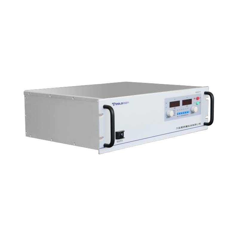
The drive power supply design must support the compensation techniques. For bipolar operation, the power supply must be capable of generating both positive and negative voltages. The voltage transitions must be fast enough to enable effective charge cancellation. For adaptive control, the power supply must provide precise voltage adjustment capability and must interface with the monitoring system.
The voltage waveform shape affects the charge injection behavior. Square wave signals with sharp transitions may cause more charge injection than signals with slower transitions. The rise and fall times of the voltage transitions affect the electric field dynamics and the charge injection rate. Optimizing the waveform shape can reduce charge injection while maintaining acceptable switching speed.
Temperature affects the charge injection and detrapping processes. Higher temperatures generally accelerate detrapping, reducing the accumulated charge. However, higher temperatures may also affect the switch mechanical properties and the dielectric characteristics. The compensation techniques must account for the temperature dependence of the charge injection behavior.
Long-term reliability testing characterizes the charge injection effects and validates the compensation techniques. Accelerated life testing subjects the switch to many switching cycles under various conditions. The drift in actuation voltage and the occurrence of stiction events are monitored. The test results guide the optimization of the drive power supply and the compensation algorithms.
Integration with the RF system requires attention to the interaction between the drive circuit and the RF signal path. The drive voltage must not couple into the RF signal, as this would degrade the switch isolation and insertion loss. The drive circuit layout must minimize parasitic capacitance to the RF path. The compensation techniques must not introduce noise or spurious signals that could affect the RF performance.