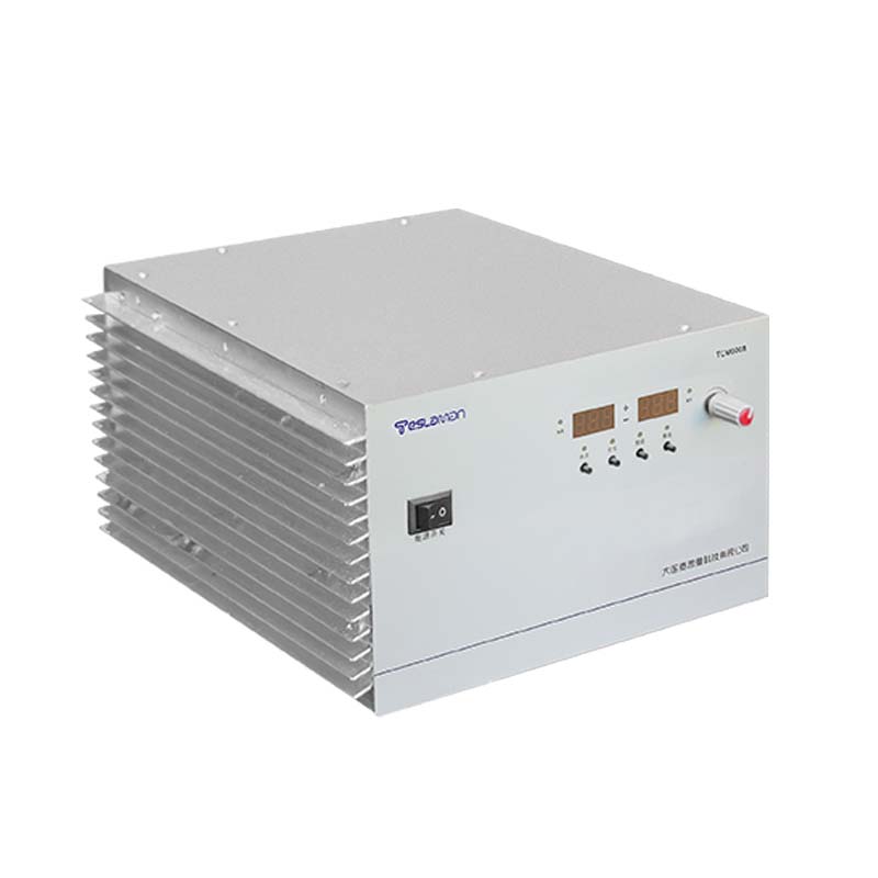
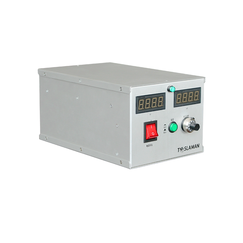
Precision Control and Process Optimization of High Voltage Transfer Printing Power Supply for Flexible Electronics Manufacturing
Flexible electronics represent an emerging technology that combines electronic functionality with flexible substrates, enabling applications from wearable devices to flexible displays. Transfer printing is a key manufacturing technique that transfers prefabricated devices from a donor substrate to a flexible receiver substrate. High voltage can assist the transfer process through electrostatic forces. Precision control of the high voltage power supply is essential for successful transfer printing.
Transfer printing uses a stamp to pick up devices from a donor substrate and print them onto a receiver substrate. The pick up and print steps require controlled adhesion between the stamp and the devices. The adhesion must be strong enough for pick up but releasable for printing. Various methods control the adhesion, including kinetic control, surface energy control, and electrostatic control.
Electrostatic transfer printing uses an electric field to control the adhesion. A voltage applied between the stamp and the substrate creates an electrostatic attraction that assists the pick up. Reversing or removing the voltage releases the devices for printing. The electrostatic force depends on the voltage, the geometry, and the dielectric properties of the intervening materials.
The high voltage power supply for electrostatic transfer printing must provide precise, controllable output. The voltage level determines the electrostatic force. Too low a voltage may not provide sufficient force for reliable pick up. Too high a voltage may cause unwanted effects such as dielectric breakdown or damage to the devices. The optimal voltage depends on the device size, the stamp geometry, and the materials.
Voltage control precision affects the transfer yield and alignment accuracy. The voltage must be set accurately to achieve the desired force. Variations in voltage cause variations in the transfer process, reducing yield. The power supply must provide stable output with minimal ripple. The setting resolution must be fine enough for process optimization.
Timing control coordinates the voltage application with the mechanical motion of the stamp. The voltage must be applied at the correct time relative to the stamp contact and separation. The timing precision affects the transfer success. The power supply must respond quickly to timing commands. The control system must synchronize the voltage with the motion system.
Polarity control enables bidirectional electrostatic forces. Positive voltage creates attraction in one direction. Negative voltage can create repulsion or attraction in the opposite direction. The ability to switch polarity enables more sophisticated control of the transfer process. The power supply must provide bipolar output or be capable of switching the output connections.
Process optimization finds the voltage and timing parameters that maximize the transfer yield and device functionality. Design of experiments systematically varies the parameters and measures the outcomes. The optimization considers the transfer yield, the alignment accuracy, and the device performance after transfer. The optimal parameters may differ for different device types and materials.
The stamp design affects the electrostatic transfer. Conductive stamps can have voltage applied directly. Dielectric stamps require electrodes patterned on or embedded in the stamp material. The stamp geometry affects the electric field distribution and the force uniformity across the stamp area.
The device and substrate materials affect the electrostatic behavior. The dielectric properties determine the capacitance and the force for a given voltage. The conductivity affects the charge distribution and the response time. The materials must be compatible with the voltage levels used to avoid damage.
Scale up from laboratory to production requires maintaining the precision and control as the process scales. Larger stamp areas may require higher currents to charge the larger capacitance. Higher throughput may require faster voltage transitions. The power supply design must accommodate the production scale requirements while maintaining the necessary precision.