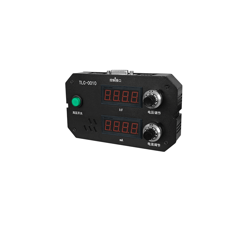
Low Noise Design and Electromagnetic Shielding of High Voltage Power Supply for Microchannel Plate Detector
Microchannel plate detectors amplify electron, ion, and photon signals through a cascade of secondary electron multiplication in microscopic channels, achieving gains of millions with subnanosecond timing resolution. These detectors serve in mass spectrometry, particle physics, imaging, and space instrumentation where signal fidelity is paramount. The high voltage power supply that biases the microchannel plate must exhibit exceptionally low noise to preserve the detector resolution and sensitivity. Electromagnetic shielding prevents interference from the power supply from corrupting the sensitive detector signals.
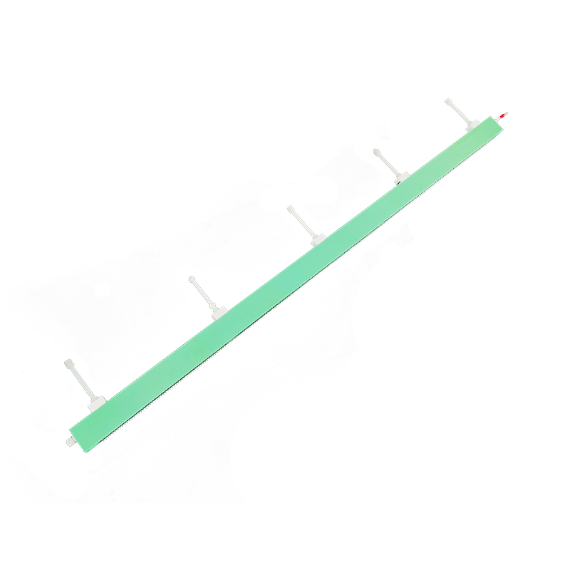
The microchannel plate consists of a thin plate containing millions of parallel channels, each functioning as an independent electron multiplier. Electrons entering a channel strike the channel wall, releasing secondary electrons that cascade down the channel, producing an output pulse of millions of electrons from a single input electron. The gain depends exponentially on the applied voltage and the channel length to diameter ratio. Typical operating voltages range from one to two kilovolts for a single plate, with two plates in chevron configuration providing higher gain.
Noise on the high voltage bias affects the detector performance through several mechanisms. Voltage fluctuations modulate the gain, causing pulse amplitude variations that degrade the energy resolution in spectroscopy applications. High frequency noise can couple to the detector output, corrupting the signal or creating spurious counts. Low frequency drift causes the gain to change over time, affecting the stability of measurements. The noise requirements are stringent because the detector amplifies signals by factors of millions, also amplifying any noise that couples to the input.
Low noise design of the high voltage power supply begins with the voltage reference, which sets the output accuracy and stability. Temperature compensated zener diodes or bandgap references provide stable references with low noise. The reference noise is amplified by the feedback loop to the output, making reference selection critical. Low noise operational amplifiers in the control circuitry minimize the contribution of amplifier noise to the output.
The high voltage generation stage typically uses a switching converter for efficiency, but switching creates noise at the switching frequency and its harmonics. Post regulation with linear regulators can reduce the switching noise at the cost of additional power dissipation. Careful design of the switching frequency and filtering can place the switching noise outside the bandwidth of interest for the detector application. Multi phase interleaved converters spread the switching noise across multiple frequencies, reducing the peak noise at any single frequency.
Output filtering attenuates the noise from the generation stage before it reaches the detector. LC filters provide low pass filtering, with the cutoff frequency set well below the switching frequency. Multiple filter stages provide greater attenuation. The filter components must be selected for low noise characteristics, with some capacitor types exhibiting microphonic noise under vibration. The filter design must also maintain stability of the feedback loop that regulates the output voltage.
Electromagnetic shielding contains the interference generated by the power supply and protects the supply from external fields. The switching converter generates magnetic fields from the inductor and current loops, and electric fields from the switching nodes. Metallic enclosures provide electric field shielding, while magnetic materials provide magnetic field shielding. The shielding effectiveness depends on the material conductivity and permeability, the enclosure geometry, and the frequency of the interference.
Cable routing and connector design affect the interference coupling between the power supply and the detector. The high voltage cable carries the bias to the detector, and any noise on the cable appears directly at the detector. Shielded cables with the shield connected to a clean ground minimize pickup. The connector design must maintain the shielding integrity through the connection, with appropriate shielding contacts and minimal exposed conductor length.
Grounding strategy prevents ground loops that can couple noise into the detector signals. The power supply ground, the detector ground, and the signal processing ground must be connected in a way that prevents noise currents from flowing through signal reference paths. Star grounding, where all grounds connect at a single point, prevents ground loops. The implementation requires careful attention to the physical layout and the cable connections.
Testing and characterization of the power supply noise performance verifies that the design meets the detector requirements. Output noise measurement with a high impedance voltmeter or spectrum analyzer quantifies the noise voltage across the frequency range. Load regulation testing measures the output variation with changing load current. Temperature coefficient measurement characterizes the output drift with temperature. These tests confirm that the power supply performance supports the detector specifications.