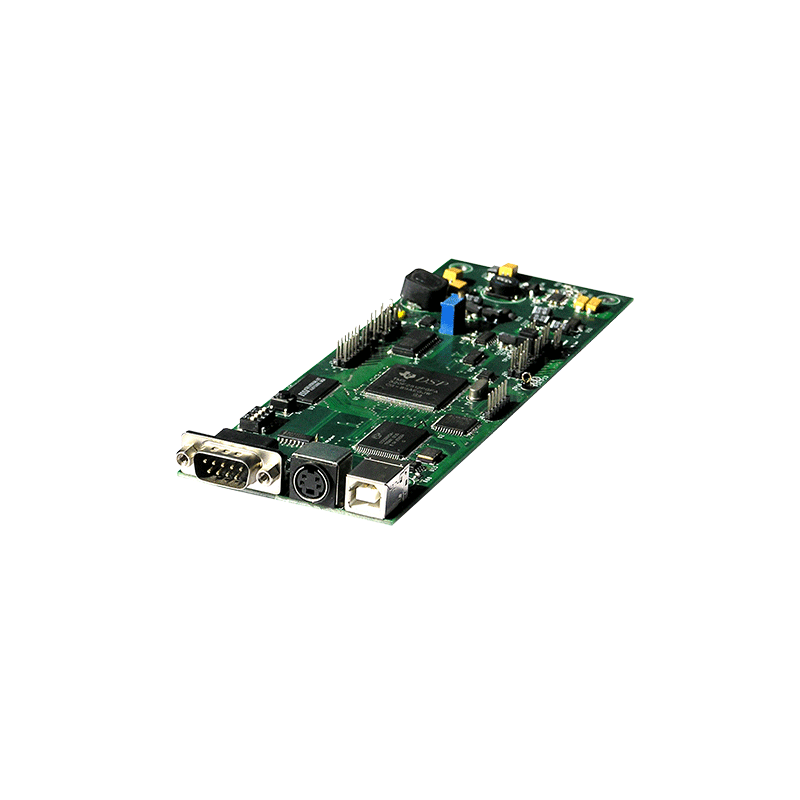
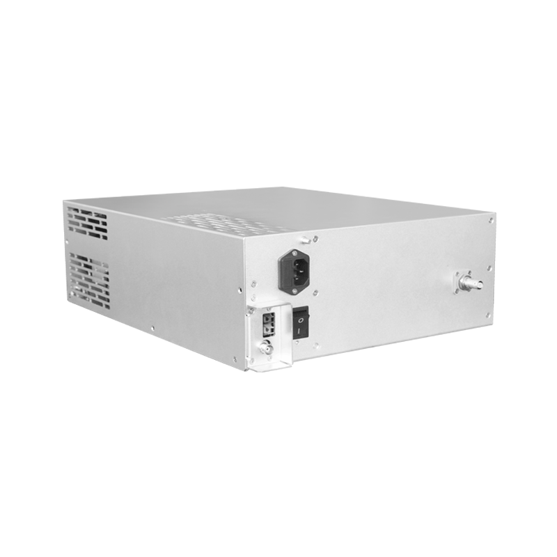
Electrostatic Chuck High Voltage Power Supply Insulation Performance Test in Vacuum Environment
Electrostatic chucks provide essential wafer holding capability in semiconductor processing equipment through the application of high voltage to embedded electrodes that generate electrostatic attractive forces. The high voltage power supply systems that bias these electrodes must maintain reliable insulation performance under vacuum conditions where electrical breakdown mechanisms differ fundamentally from atmospheric environments, necessitating comprehensive testing protocols to verify insulation integrity and operational safety. The unique characteristics of vacuum environments create specific challenges for insulation testing that require specialized equipment and procedures.
The operating principle of electrostatic chucks relies on the Coulomb force between charged electrodes and induced charges in workpiece materials, typically requiring applied voltages in the range of 500 to 3000 volts. The electrostatic attractive force increases with applied voltage, enabling adjustment of clamping force to match process requirements. However, excessive voltage can cause electrical breakdown through the chuck insulation or along surface paths, potentially damaging sensitive wafers and processing equipment. Proper insulation design and testing ensure safe operation within voltage limits appropriate for specific chuck configurations and process conditions.
Vacuum environments fundamentally alter electrical breakdown behavior compared to atmospheric conditions. At pressures corresponding to semiconductor process vacuum levels, typically in the range of 1 to 1000 Pascals, the mean free path of electrons becomes comparable to electrode gap dimensions, enabling efficient ionization cascades that lead to breakdown at lower voltage gradients than atmospheric conditions. This phenomenon, known as the Paschen minimum, creates voltage holdoff limitations that constrain electrostatic chuck operation and require specialized insulation design approaches for vacuum applications.
Insulation materials for electrostatic chuck applications must satisfy multiple requirements including high dielectric strength, low dielectric absorption, thermal stability, chemical resistance, and compatibility with semiconductor process environments. Ceramic materials, particularly aluminum oxide and aluminum nitride, provide excellent electrical insulation properties combined with good thermal conductivity essential for temperature control during processing. Polymer materials including polyimide and fluoropolymer formulations offer flexibility and ease of fabrication advantages, though with lower thermal conductivity and potential outgassing concerns in vacuum applications. Material selection for specific chuck designs depends on operating conditions, process requirements, and reliability targets.
Testing protocols for insulation performance in vacuum environments address multiple failure mechanisms including volume breakdown through insulation materials, surface flashover along insulation interfaces, and tracking degradation from cumulative discharge events. Volume breakdown testing applies increasing voltage across insulation samples until failure occurs, determining the ultimate dielectric strength of insulation materials under relevant environmental conditions. Surface flashover testing evaluates voltage holdoff along insulation surfaces where contamination, absorbed moisture, or geometric factors can create preferential discharge paths. Tracking resistance testing subjects insulation materials to repeated discharge events that simulate operational stress conditions, evaluating long-term degradation mechanisms that could cause premature failure.
Partial discharge measurement provides sensitive detection of localized insulation defects before they progress to complete breakdown. Partial discharges occur at locations where electric field stress exceeds local dielectric strength, creating small discharge events that may not immediately cause system failure but indicate developing insulation problems. Detection of partial discharge activity during insulation testing identifies potential reliability issues and guides design improvements to eliminate field concentration or insulation defects. Partial discharge measurement in vacuum environments requires specialized techniques to distinguish actual discharges from measurement artifacts caused by the vacuum environment itself.
High voltage endurance testing evaluates insulation performance under extended operation at elevated voltage levels, simulating the cumulative stress experienced during equipment lifetime. Endurance testing protocols apply voltage at specified levels for extended durations, typically hundreds or thousands of hours, monitoring insulation characteristics throughout the test period. Degradation mechanisms including thermal aging, partial discharge erosion, and chemical changes progress during endurance testing, providing data for lifetime estimation and maintenance scheduling in actual equipment operation.
Environmental conditioning of insulation test samples simulates the thermal and chemical exposure experienced during processing operations. Temperature cycling tests evaluate insulation stability under thermal excursions that occur during heating and cooling cycles of processing sequences. Chemical exposure testing subjects insulation materials to process gases and cleaning agents encountered in actual equipment operation, evaluating resistance to chemical attack that could degrade insulation performance. Combined environmental testing addresses interactions between thermal, chemical, and electrical stress mechanisms that can accelerate degradation beyond predictions from individual stress testing.
Measurement systems for insulation testing in vacuum environments require specialized configurations to ensure accurate, reliable data acquisition under challenging conditions. High voltage measurement dividers with appropriate vacuum-compatible construction enable accurate voltage monitoring without introducing additional leakage paths or measurement errors. Current measurement systems detect microampere-level leakage currents that indicate developing insulation problems, with sufficient sensitivity and noise immunity to distinguish true leakage from spurious signals. Vacuum-compatible cabling, connectors, and feedthroughs maintain measurement integrity while providing necessary isolation between test samples and measurement instrumentation.
Data analysis and interpretation from insulation testing programs require correlation with equipment design parameters and operational requirements to guide design optimization and operating procedure development. Statistical analysis of breakdown voltage distributions characterizes insulation performance variability that affects safety margins and reliability predictions. Failure mode analysis of failed samples identifies degradation mechanisms and design features that contribute to failure susceptibility. Application of testing results to equipment design decisions requires engineering judgment informed by understanding of material properties, failure mechanisms, and operational requirements to achieve reliable, safe equipment designs that perform consistently throughout specified equipment lifetime.
Production qualification testing for electrostatic chucks addresses the specific requirements of semiconductor manufacturing environments where wafer damage has significant economic consequences. Test protocols simulate multiple processing cycles to verify insulation reliability under representative operating conditions. Statistical sampling approaches ensure adequate confidence in population quality while maintaining practical test durations. Documentation of test results and equipment history supports quality management systems required for semiconductor manufacturing qualification.
Advanced testing techniques employing optical and acoustic detection methods enable characterization of discharge phenomena during insulation testing. Optical emission from partial discharges provides information about discharge location and intensity. Acoustic emission detection offers complementary detection capability particularly useful for identifying discharge events in opaque insulation structures. Combined measurement approaches provide comprehensive characterization of insulation behavior under electrical stress, supporting design optimization for maximum reliability in demanding semiconductor processing applications.