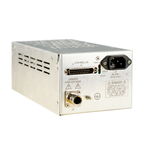
Topological Structures of High-Voltage Power Supplies for Semiconductor Testing
Abstract: This article delves into the topological structures of high-voltage power supplies for semiconductor testing, meticulously analyzing the working principles, advantages and disadvantages, as well as the application scenarios in the field of semiconductor testing for various common topological structures. It aims to provide comprehensive theoretical references and technical guidance for research and applications in related fields.
I. Introduction
With the rapid development of semiconductor technology, the performance testing of semiconductor devices has imposed increasingly higher requirements on high-voltage power supplies. The topological structure of a high-voltage power supply directly affects key performance indicators such as its output characteristics, efficiency, stability, and reliability. Therefore, selecting an appropriate topological structure is of crucial importance for semiconductor testing.
II. Common Topological Structures
(1) Linear Topological Structure
The linear topological structure is a relatively simple high-voltage power supply topology. Its basic principle is to control the output voltage by adjusting the gain of a linear amplifier. The advantages of this topological structure lie in its high output voltage accuracy and low ripple, enabling it to provide a stable DC high-voltage output. It is suitable for semiconductor testing scenarios that demand stringent voltage accuracy, such as high-precision leakage testing. However, its disadvantages are also quite prominent. Due to the linear regulation method, the power loss is relatively large and the efficiency is low. Especially when outputting high voltage and large current, a significant amount of energy is dissipated in the form of heat. This not only reduces energy utilization but also requires the installation of complex heat dissipation systems, increasing the cost and size of the system.
(2) Flyback Topological Structure
The flyback topological structure utilizes the energy storage and release characteristics of the transformer to achieve voltage transformation. When the switching tube is turned on, the transformer stores energy; when the switching tube is turned off, the transformer releases the stored energy to the output terminal, thus generating a high-voltage output. Its advantages include a relatively simple structure, low cost, and the ability to achieve electrical isolation. It is suitable for some small-sized and low-cost semiconductor testing equipment. However, the flyback topological structure has issues such as relatively low output power and poor output voltage stability and load regulation rate. It may not be able to meet the requirements in tests that demand high voltage stability.
(3) Forward Topological Structure
The forward topological structure is similar to the flyback structure, but the working mode of the transformer is different. It directly transfers energy to the output terminal when the switching tube is turned on and cooperates with appropriate rectification and filtering circuits to obtain a high-voltage output. The forward topological structure has relatively high power transmission efficiency and good output voltage stability. It can provide relatively large output power and is suitable for semiconductor testing applications that require high power and voltage stability, such as the withstand voltage testing of high-power semiconductor devices. Nevertheless, the forward topological structure requires an additional reset circuit to ensure the normal operation of the transformer, which increases the complexity and cost of the circuit.
(4) Full-Bridge Topological Structure
The full-bridge topological structure consists of four switching tubes forming bridge arms. By alternately turning on and off the switching tubes, energy conversion and transmission are achieved, and a high voltage is obtained at the output terminal. This topological structure can achieve higher output power and efficiency, has a wide range of output voltage regulation, and exhibits excellent voltage and current output characteristics. It is suitable for various complex semiconductor testing requirements, especially in occasions that demand high voltage, large current, and fast dynamic response. However, the full-bridge topological structure has a complex circuit structure, is difficult to control, imposes high performance requirements on the switching tubes, and has a relatively high cost.
III. Selection and Optimization of Topological Structures
In the actual design of high-voltage power supplies for semiconductor testing, multiple factors need to be considered comprehensively to select an appropriate topological structure. First of all, specific requirements of the test, such as the test voltage range, current magnitude, voltage accuracy, stability, and dynamic response characteristics, should be taken into account to determine the key requirements for the power supply's performance. For tests that require extremely high voltage accuracy and stability, the linear topology or an optimized forward topology may be a better choice; while for high-power testing requirements, the full-bridge topological structure has more advantages.
In addition, practical factors such as cost, size, and heat dissipation also need to be considered. For example, in some small-sized and portable semiconductor testing equipment, the flyback topological structure may be more suitable due to its simple structure and small size; while for large-scale semiconductor production testing lines, although the full-bridge topological structure has a relatively high cost, considering its high performance and reliability, it may still be the preferred solution. Meanwhile, to further optimize the performance of the topological structure, some advanced control techniques can be adopted, such as soft-switching technology and closed-loop feedback control technology, to improve the efficiency of the power supply, reduce switching losses, and enhance the stability and dynamic response ability of the output voltage.
IV. Conclusion
The topological structures of high-voltage power supplies for semiconductor testing are diverse, each with its own advantages, disadvantages, and applicable scenarios. In practical applications, it is necessary to weigh various factors according to specific testing requirements and actual conditions, select the most appropriate topological structure, and adopt reasonable optimization measures to improve the performance of the power supply so as to meet the increasingly complex and stringent requirements of semiconductor testing. With the continuous progress of semiconductor technology, research and innovation on the topological structures of high-voltage power supplies will continue to deepen, providing stronger technical support for the development of the semiconductor industry.
