Key Technologies of High Voltage Power Supply in Electron Multiplier Gain Control
1. Electron Multiplication Mechanism and High Voltage Coupling
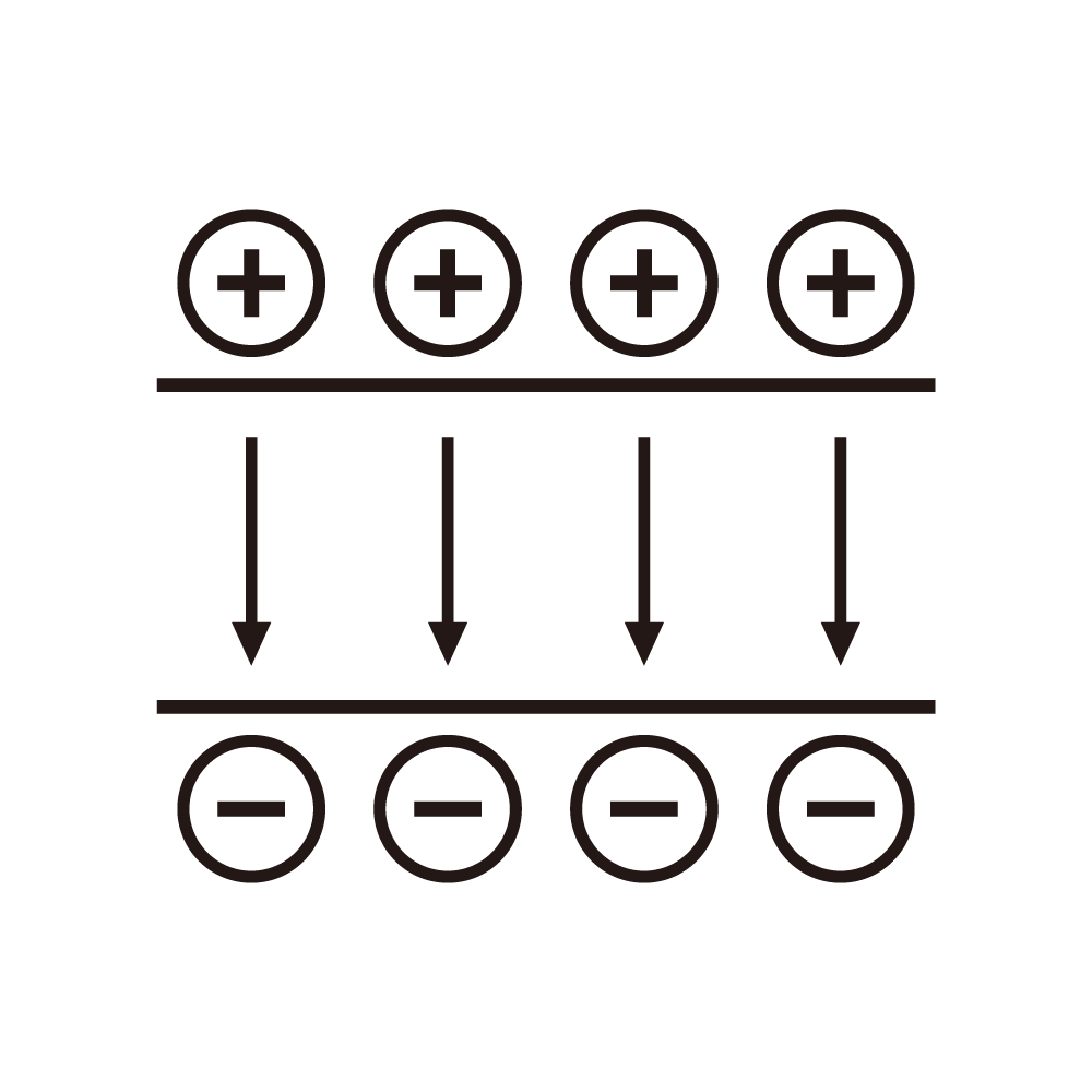
The core performance of electron multipliers relies on precise control of secondary electron emission by high voltage power supplies. With 800-1200V applied across the channels, single-electron injection triggers avalanche amplification of 10^3-10^4. Experiments show an exponential relationship between gain (G) and voltage (V) (G∝e^(kV)), where ±1% voltage fluctuation causes over 15% gain deviation. Gradient electric field design (200-300V/mm at entry, 500-800V/mm at exit) optimizes electron trajectories, reducing wall collision losses and improving gain uniformity to ±5%.
Channel geometry significantly affects gain sensitivity. For 5μm-diameter channels, 1200-1500V with ripple coefficient <0.01% is required to prevent micro-discharge-induced gain oscillation. Multi-stage voltage-divider networks limit gradient errors to 0.3%, ensuring energy transfer efficiency.
2. Critical Advancements in Power Supply Design
1. Dynamic Response Optimization
For pulsed signal detection, the supply must switch 800-1200V within 10μs. GaN-based switches (2MHz) improve response speed by 5x while reducing switching loss by 60%. Digital feedback loops (1MS/s sampling) stabilize gain fluctuation within ±0.5%.
2. Multi-Stage Gradient Configuration
Six-segment voltage division reduces total deviation to 0.05%, with 150-200V per stage. This design boosts electron transmission efficiency from 78% to 93% in MCP applications, lowering dark counts to 0.1cps/cm². Segmented insulation with alumina substrates limits leakage current to <1nA.
3. EMI Suppression
Dual-layer shielding (μ-metal + permalloy) attenuates 50kHz-1GHz EMI by >80dB. Built-in RC filters (10kHz cutoff) reduce output ripple to <1mV, ensuring >60dB SNR.
3. Systematic Process Optimization
1. Thermal Stability
Gain decreases ~2.3% per 10℃ temperature rise. Water-cooling systems (±0.1℃) with NTC compensation networks maintain gain stability <±1% across -20-50℃. Vacuum levels of 10^-5Pa limit gas collision losses to 0.8%.
2. Surface Treatment
HF etching reduces channel wall roughness (Ra) from 50nm to 8nm, increasing secondary emission coefficient (δ) from 1.8 to 2.5. ALD-coated MgO layers (10nm) reduce operating voltage by 15% while maintaining gain.
3. Pulsed Mode Optimization
Adjustable pulse widths (50ns-10ms) and duty cycles (1-50%) enable time-resolved measurements. At 1MHz repetition rates, peak current density reaches 5A/cm² with ±0.3% gain stability.
4. Technological Trends and Challenges
Distributed 16-channel modules (1mV resolution) enhance gain uniformity in large-area MCP arrays. Graphene-based cathodes reduce operating voltages below 500V while sustaining 10^4 gain. However, addressing space charge saturation at high count rates (>10^6cps) remains a critical challenge.


