Optimization of Film Compactness for Coating High-Voltage Power Supplies
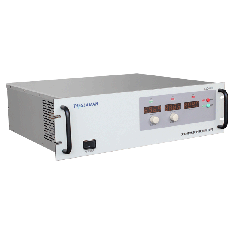
In the field of material surface treatment, coating technology is widely used in many industries such as optics, electronics, and machinery due to its advantage of endowing materials with special properties. The coating high-voltage power supply, as one of the core equipment in the coating process, plays a crucial role in the quality of the film layer, among which the compactness of the film layer is an important indicator to measure the quality of the film layer. Optimizing the relevant parameters and performance of the coating high-voltage power supply is of great significance for improving the compactness of the film layer.
The coating high-voltage power supply provides the necessary electric field environment for the coating process. Ions are accelerated under the action of the electric field and impact the target material, causing the target atoms to sputter out and deposit on the surface of the substrate to form a film layer. During this process, factors such as the stability of the output voltage and current of the power supply and the waveform characteristics have a significant impact on the compactness of the film layer.
The output voltage is one of the key parameters affecting the compactness of the film layer. If the voltage is too low, the ions do not obtain sufficient energy to fully sputter the target atoms, resulting in a slow growth rate of the film layer, and the atoms lack sufficient power to be closely arranged during deposition, thus reducing the compactness of the film layer. Conversely, too high a voltage will make the ion energy too high, which may cause excessive sputtering of the target material and generate a large number of high-energy particles. When these particles are deposited on the substrate surface, defects are likely to be formed, which is also not conducive to the improvement of the compactness of the film layer. Therefore, accurately adjusting the output voltage of the high-voltage power supply to an appropriate range is the basis for optimizing the compactness of the film layer.
The stability of the power supply output current is also crucial. Current fluctuations will lead to instability in the sputtering process, making the sputtering rate of the target atoms uneven. When the sputtering rate is fast and slow, the uniformity of atom accumulation during the growth of the film layer is destroyed, and defects such as voids and gaps are likely to appear, seriously affecting the compactness of the film layer. By adopting advanced current control technologies, such as closed-loop feedback control, to monitor and adjust the current in real-time to ensure its stable output, it helps to improve the film layer quality and increase the compactness of the film layer.
In addition, the characteristics of the output waveform of the high-voltage power supply cannot be ignored. Different waveforms, such as direct current and pulse, have different effects on the coating process and the compactness of the film layer. The pulse waveform can provide high energy in a short time, promoting the effective interaction between ions and the target material. At the same time, during the pulse interval, the substrate surface has enough time for atomic rearrangement and adjustment, which is conducive to the formation of a more compact film layer structure. Reasonable selection and optimization of the power supply output waveform can significantly improve the compactness of the film layer.
To further optimize the compactness of the film layer, other factors in the coating process can also be combined. For example, controlling the vacuum degree during the coating process, a suitable vacuum environment can reduce the interference of impurity gases on the growth of the film layer, making the atom deposition more pure and tight. At the same time, accurately controlling the substrate temperature, an appropriate temperature is conducive to the migration and diffusion of atoms on the substrate surface, promoting the orderly arrangement of film layer atoms and improving the compactness of the film layer.
In conclusion, by optimizing the key parameters such as the output voltage, current stability, and waveform characteristics of the coating high-voltage power supply, and at the same time coordinating the control of factors such as the vacuum degree and substrate temperature in the coating process, the compactness of the film layer can be effectively improved, thus providing higher-quality coated products for various industries and meeting the growing demand for material performance.