The Types of Implanted Impurities in the High-Voltage Power Supply for Ion Implantation
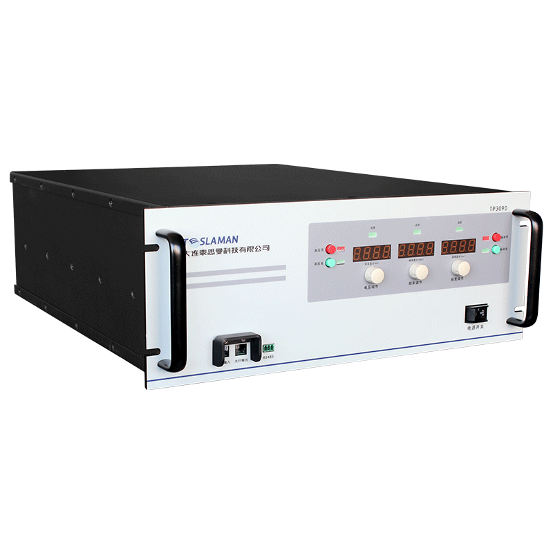
Ion implantation technology, as an important material surface modification and semiconductor manufacturing process, plays a crucial role in the field of modern technology. The high-voltage power supply for ion implantation is one of the core equipment for realizing the ion implantation process, and its performance directly affects the types of implanted impurities and the implantation effect.
In the ion implantation process, there are a variety of common implanted impurities. Among them, boron (B) is an important impurity. In semiconductor manufacturing, the implantation of boron atoms can introduce acceptor impurities into semiconductor materials such as silicon, changing the electrical properties of the semiconductor, and thus achieving precise control over the electrical performance of semiconductor devices. For example, it is used to form P-type semiconductor regions in the fabrication of integrated circuits.
Phosphorus (P) is also a commonly used implanted impurity. After phosphorus atoms, as donor impurities, are implanted into the semiconductor, the electron concentration in the semiconductor can be increased, forming an N-type semiconductor region. When manufacturing semiconductor devices such as diodes and transistors, the implantation of phosphorus plays a vital role in constructing the appropriate PN junction.
Arsenic (As) is also a frequently used impurity in ion implantation. Due to the relatively large atomic mass and suitable electronic structure of arsenic atoms, they can effectively change the carrier concentration and mobility in the semiconductor. In some high-performance semiconductor devices, such as high-speed integrated circuits and power devices, the implantation of arsenic can optimize the performance of the devices.
In addition to the above elements, some other impurities will also be implanted according to different application requirements. For example, indium (In) in some special semiconductor materials and optoelectronic devices can be used to adjust the energy band structure of the material and improve the optoelectronic performance of the device. Moreover, the implantation of light elements such as carbon (C) has also shown unique effects in some research and applications, such as increasing the hardness and wear resistance of the material.
The high-voltage power supply for ion implantation can precisely implant these different types of impurities into the specific depth and position of the target material by accurately controlling the acceleration voltage and ion beam current. This is crucial for optimizing the material performance and achieving high performance of semiconductor devices.
With the continuous development of technology, the requirements for the types of implanted impurities and the implantation accuracy in ion implantation are getting higher and higher. In the future, the high-voltage power supply for ion implantation will continue to innovate and improve to meet the implantation needs of more new types of impurities, and promote the further development of the semiconductor and materials science fields.